| Submission Procedure |
Software/Hardware Co-Design of Efficient and Secure Cryptographic HardwareNadia Nedjah Luiza de Macedo Mourelle Abstract: Most cryptography systems are based on the modular exponentiation to perform the non-linear scrambling operation of data. It is performed using successive modular multiplications, which are time consuming for large operands. Accelerating cryptography needs optimising the time consumed by a single modular multiplication and/or reducing the total number of modular multiplications performed. Using a genetic algorithm, we first yield the minimal sequence of powers, generally called addition chain, that need to be computed to finally obtain the modular exponentiation result. Then, we exploit the co-design methodology to engineer a cryptographic device that accelerates the encryption/decryption throughput without requiring considerable hardware area. Moreover the obtained designed cryptographic hardware is completely secure against known attacks. Keywords: Evolutionary Computation, Co-Design, Genetic Algorithm, Cryptography, Addition-Chain Categories: H.3.1, H.3.2, H.3.3, H.3.7, H.5.1 1 IntroductionThe modular exponentiation is a common operation for scrambling and
is used by several public-key cryptosystems, such as the RSA encryption
scheme [Rivest, 78]. It consists of a repetition
of modular multiplications: C = TE mod M,
where T is the plain text such that 0 The performance of such cryptosystems is primarily determined by the implementation efficiency of the modular multiplication and exponentiation. As the operands, i.e. the plain text of a message or the ciphertext (possibly a partially ciphered) are usually large (i.e. 1024 bits or more), and in order to improve time requirements of the encryption/decryption operations, it is essential to attempt to minimise the number of modular multiplications performed as well as the time needed to perform a single modular multiplication. Page 66 Most of the work [Blum, 99, Walter, 93, Nedjah, 02a] on improving the characteristics, i.e. encryption/decryption throughput and required resources, focus on one aspect: minimising the exponentiation time by implementing the operation on hardware. However, the proposed solutions require considerable amount of hardware area. In this paper, we propose and implement a novel solution that minimises the number of required modular multiplications along with the modular multiplication time without too much increase in resource requirements. We do so using genetic algorithms [Nedjah, 02b] and the co-design methodology [Balarin, 97]. The proposed solution finds a balance between the two requirements: time and area. Also, it allows one to change the encryption and decryption key freely without any extra cost. First, we introduce the concept of evolutionary addition chains as well as addition chain based methods to perform modular exponentiation. Then, we introduce Montgomery's Algorithm used to implement the modular multiplication. Thereafter, we describe the co-design system. Consequently, we discuss the architecture used to implement the mixed solution. Finally, we draw some conclusions based on the analysis of the system developed. 2 Addition ChainsIt is clear that one should not compute TE then reduce the result modulo M as the space requirements to store TE is Exlog2 M, which is huge. A simple procedure to compute C = TE mod M is based on the paper-and-pencil method. This method requires E-1 modular multiplications computing all powers of T : T -> T2 -> ... -> TE-1 -> TE. The paper-and-pencil method computes more multiplications than necessary. For instance, to compute T8, it needs 7 multiplications, i.e. T -> T2 -> T3 -> T4 -> T5 -> T6 -> T7 -> T8. However, T8 can be computed using only 3 multiplications T -> T2 -> T4 -> T8. The basic question is: what is the fewest number of multiplications to compute TE, given that the only operation allowed is multiplying two already computed powers of T? Answering the above question is NP-hard, but there are several efficient algorithms that can find a near optimal one. The addition chain based methods attempt to find a chain of numbers
such that the first number of the chain is 1 and the last is the exponent
E, and in which each member of the chain is the sum of two previous members.
For instance, the longest addition chain is [1, 2, 3, ... , E-2,
E-1, E]. An addition chain of length l for
an integer n is a sequence of integers [a0, a1,
a2, ... , al] such that a0
= 1, al = n and ak = ai
+ aj, 0 Computing the minimal addition chain for a given exponent is a hard problem [Nedjah, 02b, DeJong, 89]. We used genetic algorithms [Haupt, 98] to yield optimal addition chains for large exponents [Nedjah, 02b]. We showed that the addition chains obtained using the evolutionary methodology are always very much better than those used by the traditional exponentiation methods such as the m-ary methods and sliding window methods [Nedjah, 02c]. Note that for a given exponent, there exist many addition chains. As the minimal addition chains are numerically unpredictable, every computation based on it is also unpredictable and consequently the cryptographic hardware that uses this addition chain to encrypt data is completely secure. Page 67 Algorithm 1. AdditionChainBasedMethod(T, M, E) 0: let [a0=1 a1 a2 ... al=E] be an addition chain for E; 1: powers[0] = T; 2: for k := 1 to l 3: let ak = ai + aj | 1 3 Montgomery's AlgorithmOne of the widely used algorithms for efficient modular multiplication is Montgomery's algorithm [Montgomery, 85]. This algorithm computes the product of two integers modulo a third one without performing division by M. It yields the reduced product using a series of additions. Let A, B and M be the multiplicand, the multiplier and the modulus respectively and let n be the number of digits in their binary representation, i.e. the radix is 2. So, we denote A, B and M as follows:
The pre-conditions of the Montgomery algorithm are as follows:
As we use the binary representation of the operands, then the modulus M needs to be odd to satisfy the first pre-condition. Montgomery's algorithm uses the least significant digit of the accumulating modular partial product to determine the multiple of M to subtract. The usual multiplication order is reversed by choosing multiplier digits from least to most significant and shifting down. If R is the current modular partial product, then q is chosen so that R + q x M is a multiple of the radix r, and this is right-shifted by r positions, i.e. divided by r for use in the next iteration. So, after n iterations, the result obtained is R =A x B x rn mod M. A modified version of the Montgomery's algorithm is given in Algorithm 2. In order to yield the right result, we need an extra Montgomery modular multiplication by the constant 22n mod M. However, as the main objective of the use of Montgomery modular multiplication algorithm is to compute exponentiations, it is preferable to Montgomery pre-multiply the operands by 22n and Montgomery post-multiply the result by 1 to get rid of the 2n factor. Now, we concentrate on describing the implementation of the Montgomery multiplication algorithm. Page 68 Algorithm 2. MontgomeryAlgorithm(A, B, M) 0: int R := 0; 1: for i := 0 to n-1 2: R := R + ai ( B; 3: if r0 = 0 then R := R div 2 4: else R := (R + M) div 2; 5: return R; End. 4 The Co-design ArchitectureOur investigation is based on Algorithm 1, assuming that the addition chain is provided. The software approach consists of implementing the algorithm in a programming language, such as C, and executing the compiled code in a general-purpose computer. The bottleneck in the software approach is the evaluation of the modular multiplication. Therefore, we decided to move this computation to hardware in order to explore the speedup that can be achieved by a hardware implementation. From this point on, we will have a mixed implementation, in which part of the initial specification is in software and another part is in hardware. Consequently, we will have to deal with the interaction between these two subsystems. The dynamics within the co-encryption/decryption system is described in Figure 1.
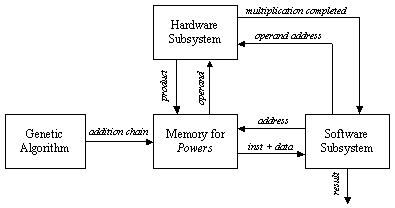
Figure 1: Dynamics within the mixed encryption/decryption process The execution cycle within the co-design system is described in the following seven steps: Page 69
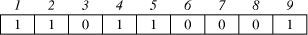
In the following sections, we explain in details, the architecture of each of the subsystems. 4.1 The Genetic AlgorithmGenetic algorithms [Haupt, 98] maintain a population of individuals that evolve according to selection rules and other genetic operators, such as mutation and recombination. Each individual receives a measure of fitness. Selection focuses on high fitness individuals. Mutation and recombination provide general heuristics that simulate the reproduction or crossover process. Those operators attempt to perturb the characteristics of the parent individuals as to generate distinct offspring individuals. The addition chain minimisation problem consists of finding a sequence of numbers that constitutes an addition chain for a given exponent. The sequence of numbers should be of a minimal length. This problem is NP-complete that is why genetic algorithms are perfect to minimal addition chains. Encoding of individuals is one of the implementation decisions one has to take in order to use genetic algorithms. It very depends on the nature of the problem to solve. There are several representations that have been used with success: binary encoding which is the most common mainly because it was used in the first works on genetic algorithms, represents an individual as a string of bits; permutation encoding, mainly used in ordering problem, encodes an individual as a sequence of integers; value encoding represents an individual as a sequence of values that consist of an evaluation of some aspect of the problem [DeJong, 89, Haupt, 98]. In our implementation, an individual represents an evolutionary addition chain. We use the binary encoding wherein 1 implies that the entry number is a member of the addition chain and 0 otherwise. Let n = 9 be the exponent. The encoding of Figure 2 represents the addition chain [1, 2, 4, 5, 9]:
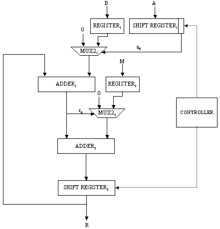
Figure 2: Addition chain encoding Page 70 4.2 Software Subsystem ArchitectureIn Algorithm 2, the formal parameters can be of 1024 bits. Therefore, instead of passing these values, we decided to pass the indexes to the array powers (i, j and k), together with the address of M and that of powers. Parameter size is related to the size of the operands. Algorithm 3 below shows the modified version of Algorithm 1. Algorithm 3. ModAdditionChainBasedMethod(T, M, E) 0: let [a0=1,a1,a2,...,al=E] be an addition chain for E; 1: powers[0] := T; 2: for k := 1 to l 3: find k | i<k and j<k, ak = ai + aj; 4: ModifiedMontgomery(i, j, k, M, powers, size); 5: return powers[l]; End. In order to perform the chosen computation, the hardware subsystem needs the function's parameters, which are sent by the software subsystem. Integer and pointer parameters are passed via memory-mapped registers, while data arrays are stored in the shared memory. Algorithm 2 must be modified as well, so as to include the necessary hardware interaction, which can be seen in Algorithm 4 below: Algorithm 4. ModifiedMontgomery(i,j,k,&M,&powers, size) 0: char* const parameter0 := (char*) 0xF000; 1: char* const parameter1 := (char*) 0xE000; 2: char* const parameter2 := (char*) 0xD000; 3: char** const parameter3 := (char**) 0xC000; 4: char** const parameter4 := (char**) 0xB000; 5: *parameter0 := i; *parameter1 := j; 6: *parameter2 := k; 7: if k = 1 then 8: *parameter3 := &M; 9: *parameter4 := &powers; 10: *parameter5 := size; 11: start(); 12: waitForInterruption(); 13: acknowledge(); End. As can be seen from Algorithm 4, parameter0, parameter1, parameter2, parameter3, parameter4 and parameter5 contain the addresses of the parameter registers located in the hardware subsystem. After their initialisation, the hardware subsystem can be started to execute the computation. In our case, parameters i, j and k are used to address the elements of the array powers, while parameter powers holds the address of the first element of the corresponding array. Hence, i, j and k are used as displacement within the array area. Since M can be large, we decided to keep M in the shared memory and pass its address only. Notice that it is up to the hardware subsystem to get the necessary data from the shared memory, once it is started. The software subsystem, then, waits for an interrupt from the hardware subsystem, indicating it has completed the operation. Page 71 4.3 Hardware Subsystem ArchitectureThe hardware subsystem comprises the hardware function and the interface logic. The latter deals with the communication between the hardware subsystem and the other entities, i.e. software subsystem and the shared memory. The characteristics of the interface depend closely on the implementation platform. Therefore, we will deal with it in the next section. The hardware function computes the modular product of two given operands using Montgomery's algorithm described in Section 3. Figure 3 shows the architecture of an iterative implementation [Nedjah, 02a] for the Montgomery modular multiplication method [Montgomery, 85]. The values of A and B are obtained from the memory, where the array elements are stored, using parameters i and j, respectively. These indexes are provided by the software subsystem. The obtained modular product is stored in the same array powers in entry k = i + j. Figure 3: Montgomery multiplication hardware Page 72 The first multiplexer of the proposed architecture, i.e. MUX21, passes 0 or the content of register B depending on whether bit a0 indicates 0 or 1 respectively. The second multiplexer, i.e. MUX22 passes 0 or the content of register M depending on whether bit r0 indicates 0 or 1 respectively. The first adder, i.e. ADDER1, delivers the sum R + ai x B (line 2 of Algorithm 2), and the second adder, i.e. ADDER2, yields the sum R + M (line 4 of the same algorithm). The shift register SHIFT REGISTER1 provides the bit ai. At each iteration i of the multiplier, this shift register is right-shifted once, so that the least significant bit of SHIFT REGISTER1 contains ai. The role of the controller consists of loading A, B and M and synchronising the shifting and loading operations of SHIFTREGISTER1 and SHIFTREGISTER2, and controlling the number of necessary iterations. Furthermore, embedded into the controller hardware, we find the steps for parameter passing as well as the handshake protocol between the hardware and software subsystems. The handshake control register signals the start (start) and parameter passing (parameters) commands from the software subsystem, and the done (done) command from the hardware subsystem. In order to synchronise the work of the components of the architecture, the controller is implemented as a state machine, which has 10 states defined as follows: Page 72 S0: Initialise state machine;
S1: If start = 0 then Go to S2 Else Go to S1;
S2: done := 0;
If start = 1 then Go to S4
Else If parameters = 0 then Go to S2;
S3: If parameter0 then Load i into REGISTERi
Else If parameter1 then Load j into REGISTERj
Else If parameter2 then Load k into REGISTERk
Else If parameter3 then
Load &M into REGISTERM
Else If parameter4 then
Load &powers into REGISTERP;
Else If parameter4 then
Load sise into counter;
Go to S2;
S4: Load powers[i] from memory into SHIFT REGISTER1;
S5: Load powers[j] from memory into REGISTER1;
S6: If k = 1 then
Load M from memory into REGISTER2;
S7: Wait for ADDER1; Wait for ADDER2;
Decrement counter;
S8: Load partial result into SHIFT REGISTER2;
S9: Enable SHIFT REGISTER2; Enable SHIFT REGISTER1;
If counter = 0 then Go to S10 Else Go to S7;
S10: Load SHIFT REGISTER2 into memory powers[k];
done := 1; Go to S1
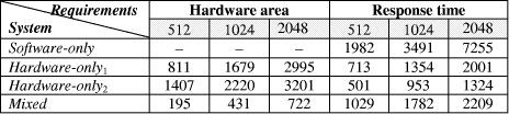
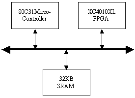
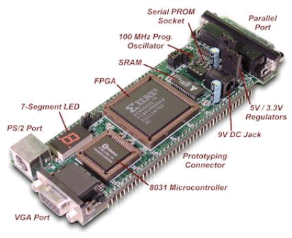
Memory read operations (to obtain the values of A, B and M) as well as memory write operations (to store the modular products) are embedded in the specification of the hardware subsystem and performed by the interface logic. Page 73 The interface between the hardware function and the software subsystem uses a control register CR through which a handshake protocol is implemented. When the software subsystem wants to call the hardware function, it asserts the start bit of CR (line 11 in Algorithm 4). When the hardware function completes the execution, it asserts the done bit of CR. When the software subsystem acknowledges the end of the hardware function operation (line 13 in Algorithm 4), it withdraws the start command by resetting the start bit of CR. When the interface logic detects that the start bit was reset, it resets the done bit, thus completing the handshake. 5 Implementation PlatformIn order to obtain a final implementation, we need a processor capable of executing the software instructions (software subsystem) and a hardware device capable of executing the chosen computation (hardware subsystem). Our co-design platform consists of the XS40 board, from Xess [Xess, 03], which is based on the Intel 80C31 micro-controller, the XilinxTM XC4010XL FPGA [Intel, 03] and 32KB of SRAM, shared by the hardware and the software subsystems. A simplified version of the co-design architecture is seen in Figure 4 and the XS40 co-design board is shown in Figure 5. Figure 4: Co-design system architecture While the hardware subsystem is computing the required modular product (computation of line 4 in Algorithm 3), the micro-controller finds the entries of array powers in which operands of the next modular multiplications (computation of line 3 in Algorithm 3) are located. Interleaving the work of the hardware function with that of the micro-controller improves a great deal the overall performance of the encryption/decryption co-design system. Page 74 Figure 5: XilinxTM XS40 co-design board 6 Timing and Area CharacteristicsIn this section, we compare the proposed cryptographic hardware, which is a mixed system (i.e. software and hardware) described throughout this paper with the software-only and hardware-only versions. The software-only system is implemented in ASM51 assembly language [Xilinx, 03]. Recall that the software subsystem of the proposed solution is also implemented using ASM51. The two hardware-only systems are implemented into XS4000: the first system is based on the binary exponentiation method and the second on the m-ary exponentiation method [Mourelle, 04], which is a generalisation of the binary method as instead of considering windows of one bit, the m-ary method deals with windows of m bits. Recall that the hardware subsystem of the mixed system is also implemented into the same FPGA family. The software-only and one of the hardware-only implementations are based on the binary modular exponentiation. The latter implementation was developed by the authors (see [Nedjah, 02a]). In the following, we briefly describe the binary method and the hardware architecture of the first hardware-only system and thereafter, we introduce the m-ary exponentiation method together with the hardware architecture of the second hardware-only implementation. Interested author can find more details about both hardware implementations in [Nedjah, 02a, Nedjah, 03, Mourelle, 04]. Page 75 6.1 Binary exponentiation-based implementationThe binary exponentiation algorithm is given in Algorithm
5, wherein k is the number of digits in exponent E, T
is the text to be encrypted/decrypted and M as before is the modulus.
Exponent E consists of its binary representation Algorithm 5. BinaryExponetiation(T, E, M) 0: int C; 1: if ek-1 = 1 then R := T else R := 1; 2: for i := k-2 downto 0 3: C := C ( C mod M; 4: if ei = 1 then C := C x T mod M; 5: return C; End. Hence the addition chain used by the binary method is as follows, wherein
identical members must be discarded. For instance for exponent E
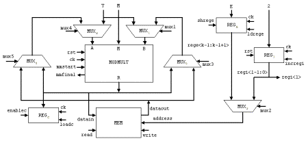
= 250 = 11111010, the addition chain will be [ek-1, 2ek-1, 2ek-1+ek-2, ... , 2(2(...2(2(2ek-1+ek-2)+ek-3)+...))+e1+e0] The architecture of the hardware [Nedjah, 03] that performs the binary exponentiation is shown in Figure 6. It uses two modular multipliers whose architectures are that shown in Figure 3 and a controller that determines the sequence of event. When the iteration finishes the controller halts and the result is found in register MPRODUCT. The first multiplier, i.e. MULTIPLIER1 performs the squaring of line 3 in Algorithm 5 while the second multiplier, i.e. MULTIPLIER2 performs the multiplication of line 4 in Algorithm 5, when it is necessary. 6.2 M-ary exponentiation-based implementationGenerally speaking, the m-ary methods for exponentiation [1] may be thought of as a three major steps procedure: (i) partitioning the binary representation of the exponent E in k-bit windows; (ii) pre-computing all possible powers in windows one by one; (iii) iterating the squaring of the partial result k times to shift it over, and then multiplying it by the power in the next window, if the window is different from 0. In other words, the m-ary methods scans the digits of E from the less significant to the most significant digit and groups them into partitions of equal length log2m, where m is a power of two. Note that 2-ary method coincides with the binary exponentiation methods described earlier (Algorithm 5). Page 76 Figure 6: Details of the architecture of binary exponentiator In general, the exponent E is partitioned into p partitions, each one containing l = log2m successive digits. If the last partition has less digits than log2m, then the exponent is expanded to the left with at most log2m - 1 zeros. The m-ary algorithm is described in Algorithm 6, wherein as before M and E represent the modulus and exponent of the cryptosystem, T and C stand for the text and the ciphertext, respectively, and, finally, Vi denotes the decimal value of partition Pi. Algorithm 6 implements the modular multiplication Montgomery's algorithm (Algorithm 2) and whose hardware architecture is given in Figure 7. Page 77 Algorithm 6. M-aryExponentition(T, M, E) 1: Partition E into p l-bit windows; 2: for i = 2 to m-1 Compute Ti mod M; 3: C := The hardware that implements the m-ary method, presented in Algorithm 6, is described in Figure 7. The first or pre-processing step (Line 2) computes all the possible powers of T, with respect to the partition size l, and stores them in a local memory (MEM). Later on, i.e. in the second or exponentiation step (Line 3 to 6), each partition of the exponent E will be used to address the memory to obtain the pre-computed power of T. Figure 7: The architecture of the m-ary hardware There is no need to store T0 mod M, since zero partitions are not considered (see Line 6 of Algorithm 6). The first power of T, i.e. T2 modulo M, is computed by passing T through both multiplexers MUX1 and MUX4, feeding the modular multiplier (MODMULT). The result is then stored in location 2 of MEM, using the initial value of register REGI. This register is responsible for generating the power memory addresses during the pre-processing step. The subsequent possible powers are obtained, successively, by passing the previous result through multiplexer MUX3 then MUX1. Note that T is kept available through multiplexer MUX4. The memory locations are generated by incrementing REGI whenever a new address is required. In each iteration of the exponentiation step, the partial result
C is raised to the 2l power then multiplied
by Page 78 In order to obtain the value of the current partition, we store exponent E in shift register REGE, from which the most significant partition is retrieved to address the power memory (see line 3 and 6 of Algorithm 1). When a new partition is required, register REGE is left-shifted l times. Recall that l represents the partition size. This operation is controlled by a down counter, initialised with l and decremented each time the register REGE is left-shifted. Signal zerol is asserted when the down counter reaches zero. The square-and-multiply loop (starting in line 5 of Algorithm 6) consists of two main phases:
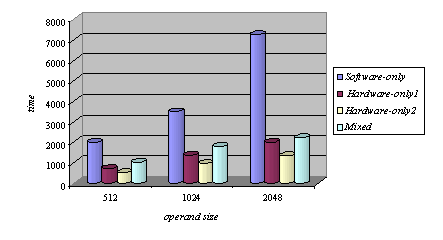
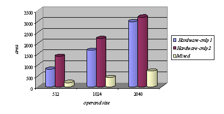
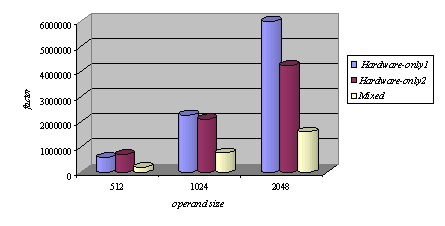
The square-and-multiply loop is performed until the least significant partition of E is reached. This is controlled by a down counter, which is initialised with p and decremented each step of the loop. Recall that p denotes the number of partitions. Signal zerop is asserted when the down counter reaches zero. The final result is, then, loaded from SHIFTREGISTER2 in the architecture of Figure 3 into register REGC. 6.3 Result ComparisonFor the four systems, i.e. the software-only, the two hardware-only and the proposed co-design systems, we obtained the hardware required, where it is applicable, as well as the response time. The obtained figures are given in Table 1. The charts of Figure 8 represent the time requirements for the three considered implementations, i.e. software-only, hardware-only and hardware/software co-design implementation. It shows clearly that the software-only has the worst time whilst the hardware-only offers the best time. Moreover, it demonstrates that the response time of the mixed implementation is not that bad with respect to the best time. The mixed implementation is about 27% slower than the hardware-only ones. Page 79 Table 1: Hardware area (CLBs), response time (ns) and performance factor under the three implementations: software-only, hardware-only and mixed system Figure 8: Comparison of the response time for the considered implementations The chart of Figure 9 represents the hardware area consumption for the hardware-only and the mixed implementations. Clearly, the co-design implementation requires very much less hardware than the hardware-only solution. The latter consumes about four times more hardware area than the former. Figure 9: Comparison of the required hardware area of the considered implementations, when applicable Page 80 The chart of Figure 10 represents the performance factor areaxtime for the implementations, which involve hardware, i.e. the hardware-only and the mixed implementations. It is clear from this chart that the co-design system improves a very great deal the performance factor. The improvement is about 65%. Figure 10: Performance factor for the hardware-only and mixed implementations 5 ConclusionIn this paper, we proposed and implement a novel solution that focuses on the two major aspects impacting on the performance of any given cryptosystems based on modular exponentiation as a non-linear function for data scrambling: (i) the proposed solution minimises the number of required modular multiplications and; (ii) the modular multiplication time, without too much increase in resource requirements. To do so, we evolve, using genetic algorithms, a minimal addition chain based on which we perform the modular exponentiation. Moreover, we exploited the co-design methodology to partition the modular exponentiation into two subsystems: the hardware subsystem and the software subsystem. Given the adequate operands, the former performs a single modular multiplication. The latter coordinates the work of the hardware subsystem based on the evolutionary addition chain. The solution proposed and implemented finds a balance between the two requirements: time and area. Furthermore, it allows one to change of the encryption and decryption key freely without any extra cost. We demonstrated that the response time of the mixed implementation is not that bad with respect to that of the hardware-only implementation. As a matter of fact, the co-design based implementation is about 27% slower than the hardware-only one. However, the mixed implementation requires very much less hardware than the hardware-only solution. The latter consumes about four times more hardware area that the former. Finally, we showed that the co-design based system improves considerably in about 65%. Page 81 References[Balarin, 97] F. Balarin et al., Hardware-software co-design of embedded systems: the polis approach, Kluwer Academic Publishers, 1997. [Blum, 99] Blum, T. and Paar C., Montgomery modular exponentiation on reconfigurable hardware, Proceedings of the 14th. IEEE Symposium on Computer Arithmetic, Australia, 1999. [DeJong, 89] DeJong, K. and Spears, W.M., Using genetic algorithms to solve NP-complete problems, Proceedings of the Third International Conference on Genetic Algorithms, pp. 124-132, Morgan Kaufmann, 1989. [Haupt, 98] Haupt, R.L. and Haupt, S.E., Practical genetic algorithms, John Wiley and Sons, 1998. [Intel, 03] Intel, MCSTM51 family of micro-controllers architectural overview, http://www.intel.com, 2003. [Montgomery, 85] P.L. Montgomery, Modular Multiplication without trial division, Mathematics of Computation 44, pp. 519-521, 1985. [Mourelle, 04] Mourelle, L.M. and Nedjah, N., Fast reconfigurale hardware for the m-ary modular exponentiation, EUROMICRO Symposium on Digital System Design: Architectures, Methods and Tools, August 31st - September 3rd., Rennes, France, 2004. [Nedjah, 02a] Nedjah, N and Mourelle, L.M., Two hardware implementations for the Montgomery multiplication: sequential vs. parallel, Proceedings of the 15th. Symposium on Integrated Circuits and Systems Design, Brazil, IEEE Computer Society, pp. 3-8, 2002. [Nedjah, 02b] Nedjah, N. and Mourelle, L.M., Minimal addition chains for efficient modular exponentiation using genetic algorithms, Proceedings of the Fifteenth International Conference on Industrial & Engineering Applications of Artificial Intelligence & Expert Systems, Cairns, Australia, Lecture Notes in Computer Science, Springer-Verlag, vol. 2358, pp. 88-98, 2002. [Nedjah, 03] Nedjah, N. and Mourelle, L.M., Three Hardware Implementations for the Binary Modular Exponentiation: Sequential, Parallel and Systolic, Proceedings of the 15th. International Symposium on Computer Architecture and High Performance Computing, São Paulo, Brazil, IEEE Computer Society Press, 2003. [Nedjah, 02c] Nedjah, N. and Mourelle, L.M., Efficient parallel modular exponentiation algorithm, Proceedings of the Second International Conference on Information Systems, Izmir, Turkey, Lecture Notes in Computer Science, vol. 2457, pp. 405-414, 2002. [Rivest, 78] Rivest, R.L., Shamir, A. and Adleman, L., A method for obtaining digital signature and public-key cryptosystems, Communication of ACM, vol. 21, no.2, pp. 120-126, 1978. [Xess, 03] Xess, http://www.xess.com, 2003. [Xilinx, 03] Xilinx, http://www.xilinx.com, 2003. [Walter, 93] C. D. Walter, Systolic modular multiplication, IEEE Transactions on Computers, 42(3):376-378, 1993. Page 82 |
|||||||||||||||||
 T < M and C is the cipher text or vice-versa, E
is either the public or the private key depending on whether T is
the plain or the cipher text, and M is called the modulus. The decryption
and encryption operations are performed using the same procedure, i.e.
using the modular exponentiation.
T < M and C is the cipher text or vice-versa, E
is either the public or the private key depending on whether T is
the plain or the cipher text, and M is called the modulus. The decryption
and encryption operations are performed using the same procedure, i.e.
using the modular exponentiation. 
 ek-1ek-2...
e1e0
ek-1ek-2...
e1e0  .
The algorithm output C is the ciphertext or plaintext depending
on whether T is the plaintext or ciphertext.
.
The algorithm output C is the ciphertext or plaintext depending
on whether T is the plaintext or ciphertext. 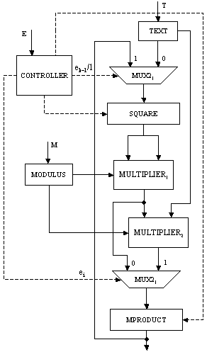
 mod M;
4: for i := p-2 downto 0 do
mod M;
4: for i := p-2 downto 0 do
 mod M;
 0 then C := Cx
 mod M;
 modulo M, when Vi is not a zero partition
(see
modulo M, when Vi is not a zero partition
(see