| Submission Procedure |
Performance Evaluation and Limitations of a Vision System on a Reconfigurable/Programmable ChipJosé Fernández-Pérez, Francisco J. Sánchez-Fernández,
Ricardo Carmona-Galán Abstract: This paper presents a survey of the characteristics of a vision system implemented in a reconfigurable/programmable chip (FPGA). System limitations and performance have been evaluated in order to derive specifications and constraints for further vision system synthesis. The system hereby reported has a conventional architecture. It consists in a central microprocessor (CPU) and the necessary peripheral elements for data acquisition, data storage and communications. It has been designed to stand alone, but a link to the programming and debugging tools running in a digital host (PC) is provided. In order to alleviate the computational load of the central microprocessor, we have designed a visual co-processor in charge of the low-level image processing tasks. It operates autonomously, commanded by the CPU, as another system peripheral. The complete system, without the sensor, has been implemented in a single reconfigurable chip as a SOPC. The incorporation of a dedicated visual co-processor, with specific circuitry for low-level image processing acceleration, enhances the system throughput outperforming conventional processing schemes. However, time-multiplexing of the dedicated hardware remains a limiting factor for the achievable peak computing power. We have quantified this effect and sketched possible solutions, like replication of the specific image processing hardware. Keywords: Image processing, System-on-a-Programmable-Chip Implementation, Algorithms Implemented in hardware [Integrated Circuits], Hardware architecture [Computer Graphics]. Categories: B.7.1, C.1.4, C.4, C.5.4, I.3.1, I.4.9 1 IntroductionHigh-speed image processing is of crucial importance in applications with critical timing. Especially in fields like autonomous robot navigation [Makimoto, 02], cruise control and collision alerts in the automotive industry [Stein, 05] and the development of ambient intelligence devices based on artificial vision [Aarts, 03]. When considering obstacle detection and object tracking in a changing environment, systems based in a single general purpose processor are not suitable for an accurate and timely response. On one side, serialized data processing is prone to limiting bottlenecks. On the other side, the microprocessor, which may not have optimized hardware for the realization of the processing tasks, has to deal with lateral tasks like communication with the peripheral devices and the execution of a global program. Therefore, the implementation of real-time image processing in highly demanding applications is not viable with serialized data processing systems. Page 440 Let us consider an image flow of 25 frames per second (fps). With a QCIF frame size, 176 x 144 pixels [ITU, 93], it means a rate of 0.63Mpixels/s. If a particular application requires the convolution of the image with 20 3x3-pixel spatial masks —what means 9 products and 8 additions of integers, once digitized—, the system should be able to develop a peak computing power of 214MOPS1. In addition, in applications like autonomous robots and portable smart cameras, strong limitations on the overall system power consumption are found. It is practically impossible to achieve, in these conditions, the required computing power with a general purpose processor —although being able of e. g. 9730MIPS2 [Intel, 04], this is done at the expense of a high clock frequency, 3.2GHz, and hence a high power consumption, 103W. In order to efficiently realize the required computing power, a feasible alternative would be the design of a specific piece of hardware. It would have the twofold mission of realizing the low-level image processing tasks at a lower cost and, besides, alleviate the central processor load. In the end, these tedious and regular tasks are the most computationally demanding part of the vision algorithm. As a natural consequence of this partition, the image processing throughput will increase. In this paper, we will evaluate the performance and limitations of a vision system consisting in a central processor, with on-chip peripherals, and a special co-processor for low-level image processing tasks. The complete system will be implemented in a Xilinx Virtex II Pro FPGA, operating at a 50MHz clock. 2 Architecture of the Vision SOPCThe architecture of the vision system developed for this project is depicted in Fig. 1. It incorporates, in a single silicon reconfigurable chip, all the components required for image processing and transmission, as well as the port for connecting to image acquisition devices. Described at the higher level, this vision SOPC is composed of:
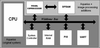
1MOPS: Millions of operations per second (additions, multiplications, etc.). 2MIPS: Millions of instructions per second. This performance index is not very accurate as some instructions may require a variable number of clock cycles and, at the same time, a single arithmetic operation may require of several instructions to be completed. Page 441 Figure 1: Block diagram of the vision system 2.1 Microcontroller UnitThe primary processor of the system (CPU) and the peripherals for data storage and exchange constitute the microcontroller unit (MCU). For the implementation of the MCU we have employed a public domain processor, Aquarius [Aitch, 03], obtained from [OpenCores, 99]. In the selection of the MCU, several factors contributed to the decision of using Aquarius. Contrarily to Xilinx Microblaze [Xilinx, 06], OpenCores offers full access to the microprocessor code. This, at an initial stage, supposes an advantage, especially when trying to implement a system that will incorporate non-conventional peripherals and whose advanced features could be based on the implementation of a dedicated architecture. When working with Microblaze, access to the internal structure of the MCU is blocked, as it is provided as an encrypted core that the CAD tools incorporate to the design as is. Other factors that contributed to the selection of Aquarius are that it is fully documented and it complies with a bus architecture intended to realize a system-on-a-chip (SoC). And, finally, it was described in Verilog [IEEE, 01]. Being part of a larger project concerning the development of vision SoC's, we sought for a processor that we could test on FPGA and incorporate later to an ASIC, using tools for IC synthesis accessible for us. The main characteristics of the selected MCU are:
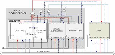
Inside Aquarius, the architecture of the buses follows WISHBONE specifications [Peterson, 02]. This allows for feasible device integration into a SoC (System-on-a-Chip). One of the main features of WISHBONE compatible buses is the standard interconnection scheme, which is based in a low number of gates. Page 442 This will simplify the interconnection between different components of the system. Therefore, the design of the interface for the visual coprocessor will be quite straightforward, while proper connection to the MCU is granted. As depicted in Fig. 1, the original Aquarius MCU contains the CPU and a set of peripherals: the system controller, the internal RAM, the parallel port (PIO) and the UART. Added to the basic system, another two peripherals have been incorporated to build our vision system: the visual co-processor and the DPRAM. Both of them are WISHBONE compatible, in order to be seamlessly allocated in the processor's address space. However, a controller for direct memory access (DMA) between the visual co-processor and the DPRAM has been implemented, as these data exchanges occur separately from the system data bus. Concerning application programming, there are cross-compilers that allow developing programs in C and translating them into SuperH-2 instructions to be executed by the vision SOPC. In our development system, the internal RAM of Aquarius is directly programmed in C. The proper initialization is realized by the hardware development tools. In a stand-alone production system, this program could be coded in an EEPROM and loaded at system boot time. 2.2 Visual Co-ProcessorThe visual co-processor (VP) has been designed to realize low-level processing on images stored in the DPRAM. They can be received from a camera or sent by a PC via the UART. The parallel I/O can also be employed for this purpose, but it will require the incorporation of some glue logic. In this first version of the system, images are received through the UART and the CPU allocates them in the image data memory (DPRAM). The VP has access to the image data through an additional port, in order not to interfere with the operation of the MCU. Fig. 2 depicts a block diagram of the internal structure of the visual processor and its main components:
Page 443 Figure 2: Internal structure of the co-processor and connections to the DPRAM Back to the diagram in Fig. 2, data buses are represented in blue while address buses are in red. The processing operators described above share the secondary port of the DPRAM. This version of the system does not contain any arbitration of these accesses. Control must be realized in software. 2.3 Dual-port RAMIn order to disengage the operation of the visual co-processor from the execution of the global program by the MCU, a dual-port RAM for the storage of image data has been implemented. Therefore, the primary port is connected to the system address and data buses while the secondary port is directly accessed by the operators of the visual co-processor. In the present version, a 64KB DPRAM has been included in the SOPC. This permits the storage of up to 16 64x64-pixel images encoded in 8-bit greyscale. Larger image sizes may require off-chip implementation of the memory, what have a negative incidence on the system performance that has not been evaluated. In order to counter these effects, arbitration techniques could be implemented to avoid collisions in the access to an external memory as proposed in [Díaz, 06]. 3 FPGA ImplementationOnce the architecture of the vision system has been established, an implementation on reconfigurable hardware will allow us to conduct different experiments. On one side, the flexibility of the FPGA implementation permits iterating the design-synthesis-test loop at zero fabrication cost. On the other side, a selection of tools integrated within the CAD environment for FPGA design, programming and debugging, will help us evaluate system performance and limitations once the functionality is tested. Page 444 3.1 Virtex II Pro Development Board and PC Host InterfaceFor the implementation of the vision SOPC, we have employed a XUPV2P board fabricated by Digilent Inc. [Xilinx, 05]. It is a development board that hosts a Xilinx Virtex II Pro FPGA, with several I/O devices and communication circuitry. Its characteristics can be summarized as follows:
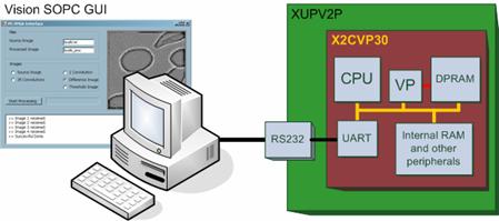
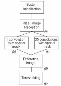
Table 1: Characteristics of the Virtex II Pro FPGAs The complete system was described in Verilog and synthesized with the help of FPGA CAD tools (Xilinx ISE 8.1). As a result of the synthesis, 30% of the available slices, 6% of the flip-flops, 27% of the LUT's and 2% of the available multipliers have been employed. The dual-port RAM has been implemented using the available BlockRAM. It is 64KB-deep and contains 8-bit-long data. The maximum allowed clock frequency is 51.618MHz. As the XUPV2P board clock is 100MHz, we will obtain a 50MHz square signal, by frequency division, to clock the vision system. Fig.3 depicts the test and development platform that we are going to use. It contains the vision SOPC in the FPGA board, which in turn communicates with a host PC employed for system programming and configuration. Image data are transmitted by the PC via RS232 and processing results are recovered through the same port. A graphical user interface (GUI) has been developed for this purpose. Results concerning system operation, speed and power are obtained from the FPGA hardware design and configuration tools. Page 445 Figure 3: Conceptual diagram of the test and development platform. 3.2 Sample ApplicationIn order to evaluate the computational cost of image processing in this architecture, we have to establish a test bench composed by the common operations required for low-level image processing. For this we will devise a simple application that makes use of these operators. This is a widely extended methodology in the characterization of embedded microprocessors [EEMBC, 97], as their peak performance is related to a vast set of parameters which, in turn, strongly depend on the particular application. Figure 4: Flow diagram of the global program of the application Page 446 The target of the image processing that we are realizing is robust edge detection on a greyscale image. It starts with a previously captured image (step (a) in Fig. 4), stored in the PC memory. It is transmitted to the vision SOPC via the PC serial port, with the help of the on-chip UART. Then, the first thing will be to eliminate imperfections due to noise in the capture and/or transmission of the image. We will employ a lowpass spatial filter based on linear diffusion of the original values of the pixels [Jähne, 99]. We will implement a discretized version, in space and time, of the following differential equation:
(1) where I(x,y) is the luminance, a function that relates each point of the image plane with its corresponding brightness. The spatial cut frequency of the lowpass filter is inversely proportional to the period of time that we allow the diffusion of the pixel values to evolve. As the diffusion in our purely digital system is discretized both in space and in time, we will control the diffusion time by the number of iterations that we realize the convolution of the original image with this spatial mask:
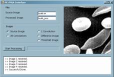
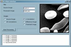
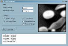
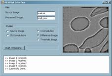
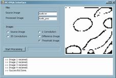
(2) which is a discrete-space approximation of the Laplacian operator. In fact, we are implementing a Forward-Euler simulation of a discrete-space approximation of the differential equations that describe linear diffusion (Eq. 1). The method for obtaining robust edge detection is suppressing all the spatial frequency components of the image that correspond to elements that are not precisely the edges of the principal elements of the scene. There are frequency components in the lower part of the spectrum that correspond to the flat area of the images. They do not represent change but the dc and near dc values. On the other extreme, there are high frequency components that correspond to spurious edges and can lead to false edge detection. In order to eliminate all the components outside a prescribed central range, bandpass filtering is required. We are going to combine two lowpass filters in order to realize a spatial bandpass filter. In the left thread of the diagram in Fig.4, the convolutions of the Laplacian mask with the original image is performed once. In the other thread it is realized 35 times. As a result, the original image (Fig.5(a)) is lowpass filtered with a high cut frequency (Fig. 5(b)) and with a lower cut frequency (Fig.5(c)). Subtracting this last image from the previous, a bandpass filtered version is obtained (Fig. 5(d)). Finally, all the pixels above a certain threshold are highlighted recognized as edges of the constitutional elements of the original scene. The resulting image, as well as the intermediate results, is sent back to the PC, via the serial port. The process can be monitored, off-line, with the help of a graphical user interface (GUI) developed for this project (Fig. 5). Page 447
Figure 5: GUI showing initial (a), intermediate (b), (c), (d) and final (e) images. 4 Performance Evaluation and Discussion4.1 System Characterization: Strengths and LimitationsOnce the functionality of the system has been throughout verified, with the help of the sample application described in the previous section, it is time to address the maximum ratings of the system. The aim of designing specific hardware for low-level image processing is to accelerate the execution of these tasks in conventional architectures. This speedup allows for real-time operation and energy efficient implementation of artificial vision. Thus, on one side, we are interested in measuring the system performance in terms of MOPS, or, indirectly, for the sake of comparison, in terms of frames per second for a particular image processing algorithm Page 448 On the other side, adaptation of the system architecture to the nature of the stimuli makes the system more efficient in terms of power consumption. Although the power required to perform some basic operations onto the image does not depends in the number of parallel data paths3, the overhead circuitry required for image partitioning and data retrieval can operate on a much reduced energy budget if carefully designed. Concerning the maximum achievable computing power, it can be derived from inspection of the design characteristics. The following table summarizes the number of clock cycles it takes in the visual co-processor to realize each different operator:
Table 2: Number of cycles per pixel per operation These figures correspond to our specific implementation of the operators. It can be objected that there could be some room for optimization, but, given the current numbers, the minimum would not be very far from what we have obtained. For instance, a pipelined implementation of the convolution unit may result in a larger hardware but can certainly improve the processing speed, at the expense of a little latency. In this specific implementation, the peak performance is developed when computing the convolution of the image with a spatial 3x3-pixel mask. This corresponds to realizing 9 multiplications and 8 additions per pixel. These 17 operations take 14 clock cycles, of 20ns each. When operating at its peak, this system develops a computing power of 60.71MOPS. The replication of the convolver will have a direct incidence in this index, boosting the system performance according to: Peak Computing Power = 60.71n MOPS (3) where n is the number of convolver blocks operating in parallel. This assertion is valid as long as there is sufficient on-chip RAM and the memory bandwidth does not generate any bottleneck [Wuytack, 99], i. e. if the limiting factors are introduced by the co-processor architecture and circuitry and not by the memory access. In order to better estimate the system limitations, let us examine its performance at the low-level processing application described in the previous section. Consider that the sensor size, the CCD or CMOS camera capturing the input image, is QCIF. If the system is to realize the 36 convolutions followed by a subtraction and a threshold binarization, it will need 511 clock cycles per pixel. This is 12.63Mcycles per frame. Using a 50MHz clock, each frame will take 253ms to be processed. The final frame rate would be 3.96fps. In order to reach a reasonable frame rate, say 25fps, we will have to replicate the convolver.
3For the same frame rate, N operators in parallel can realize the same task as 1, working at 1/N of its speed. The power consumed by each of the N operators is 1/N that of the individual operator working alone. The improvement in power efficiency is not in the realization of the operator, but in the overhead circuitry for image partitioning, data routing and memory access. Page 449 This will accelerate the operation by processing several pixels in parallel. The total frame rate will then increase at the expense of more FPGA resources being used. Table 3 displays an estimation of the enhancement in system performance and its effect in the use of resources. Table 3: Estimation of the use of FPGA resources and total frame rate Observe that the number of multipliers equals the number of convolvers plus two extra multiplications. Those are required for scaling the image incremental update after convolution and the result of the subtraction to fit into the 8-bit grayscale. There are multipliers left to be used that could be employed for parallelizing the operation inside the convolution block. However, access to image data would easily become the main limiting factor in the convolver operation. For the current design, the practical limit occurs when implementing 23 convolvers operating in parallel. This will occupy the 100% of the FPGA logic slices and end up in a total frame rate of 69.56fps. Concerning the power consumption, it has been estimated using the Xpower power analysis tool of the CAD software (it is integrated in Xilinx ISE 8.1). The total estimated power consumption for this design is 421mW. This means that the vision SOPC is able of 0.144MOPS/mW. But these figures should be contrasted with direct measurement because of the limitations of the Xpower tool. This program overestimates the static power consumption related with leakage [Elleouet, 04], which in this design is hiding the real consumption that could be assigned to the vision SOPC. We are not able to compute, by means of this software, the power consumption of an individual convolver. In fact, synthesizing the convolver alone leads to quite similar figures that those of the complete system. Let us assume, as a rough and conservative estimation, that the SOPC with 23 convolvers operating in parallel, the practical limit with this FPGA, consumes 1W. As the peak computing power is of 1396.3MOPS, following Eq. (3), the vision SOPC with 23 convolvers will be capable of 1.40MOPS/mW. This performance index can be compared with that of the last breed fixed-point DSPs, capable of 5760MIPS employing 2.15W [TI, 06]. They rate 2.68MOPS/mW. It means that our vision SOPC is not far from what is already available with state-of-the-art digital signal processing, considering that these operators are not optimized and that there is necessary overhead required for the FPGA to be configured and running. As an additional observation, power savings related with the implementation of an adapted architecture come from the reduction in the effort dedicated to image partitioning and reordering. An extreme case would be to incorporate a processor at each memory location, what does not require any data transfers and reordering. Page 450 4.2 Guidelines for the Design of a Vision SoC/SOPCSeveral guidelines can be extracted from these experiments and the study on the limitations of the implementation of a vision system in a programmable chip:
5 ConclusionsGiven the capabilities of reconfigurable computing systems to implement both conventional and alternative goal-oriented architectures, we have tested the feasibility of tailoring an FPGA-based system to realize high and low-level vision processing tasks. The motivation is clear; this can represent a competitive solution for the development of low cost artificial vision systems. Especially when, the performance and limitations of this system being characterized, the hardware resources available in medium size FPGA's render quite promising figures for processing speed under a tight power budget. Our conclusions are that, based on the results of these experiments, the implementation of a complete vision system, excluding the image sensor, in a reconfigurable/programmable chip is a cost effective alternative to conventional and DSP-based approaches. On one side, the available computing power per mW is of the same order, while the flexibility of the hardware permits further optimization and adaptation to the specific vision application. On the other, the extra design effort employed in devising an adapted architecture is alleviated by the endless possibilities of design testing and refining at no fabrication cost. Page 451 Acknowledgements The authors would like to thank Santiago Sánchez-Solano, Luis Carranza-González and Carlos Domínguez-Matas for their useful directions in the physical implementation of the vision system. This work has been partially funded by project FIT-330100-2005-162 of the Spanish Ministry of Industry, Tourism and Commerce. The work of F. J. Sánchez-Fernández is supported by a grant of the Spanish Ministry of Education and Science. References[Aarts, 03] Aarts E., Roovers R., "IC Design Challenges for Ambient Intelligence", Design, Automation and Test in Europe, pp. 2-7, Munich, Germany, March 2003. [Aitch, 03] Aitch T., A Pipelined RISC CPU: AQUARIUS. Rev. 1.1, July 2003. [EEMBC, 97] The Embedded Microprocessor Benchmark Consortium 1997-2006, http://www.eembc.org [Elleouet, 04] Elleouet D., Julien N., Houzet D., Cousin J.-G., Martin M., "Power Consumption Characterization and Modeling of Embedded Memories in XILINX". Proc. of the Euromicro Symposium on Digital System Design (DSD 2004), pp.394-401, 31 Aug.-3 Sept. 2004. [Díaz, 06] Díaz J., Ros E., Mota S. and Rodriguez-Gomez R., "Highly paralellized architecture for image motion estimation", Lecture Notes in Computer Science, Springer-Verlag, Vol. 3985, pp. 75-86, 2006. [IEEE, 01] IEEE standard Verilog hardware description language, IEEE Std 1364-2001, 2001 [Intel, 04] Intel® Pentium® 4 Processor on 0.13um Process Datasheet. Document No.: 298643-012, February 2004. [ITU, 93] Rec. H. 261: Video Codec for Audiovisual Services at p x 64kbit/s. Rec. ITU, Helsinki, 1993. [Jähne, 99] Jähne B., Haußecker H., Geißler P.(Eds.), Handbook of Computer Vision and Applications, Vol.2. Academic Press, San Diego, 1999. [Makimoto, 02] Makimoto T., Doi T.T., "Chip Technologies for Entertainment Robots". International Electron Devices Meeting, pp. 9-16, December 2002. [OpenCores, 99] OPENCORES.ORG 1999-2006, http://www.opencores.org [Peterson, 02] Peterson W.D., Specification for the WISHBONE SoC Intercconection Architecture for Portable IP Cores. Rev. B. 3. September 2002. [Renesas, 04] Renesas Technology. SH-1/SH-2/SH-DSP Software Manual, Rev. 5.00, June 30, 2004. [Stein, 05] Stein G.P. et al., "A Computer Vision SoC: a Case Study from the Automotive Domain". IEEE Computer Society Conference on Computer Vision and Pattern Recognition, Vol. 3, pp.130-134, June 2005. [TI, 06] Texas Instruments, Video and Imaging Solutions Guide, 2Q, 2006. Page 452 [Wuytack, 99] S. Wuytack S. et al. "Minimizing the Required Memory Bandwidth in VLSI System Realizations", IEEE Transactions on VLSI Systems, Vol.7, No.4, pp.433-441, December 1999. [Xilinx, 05] Xilinx University Program, Virtex-II Pro Development Syst. Hardware Ref., Ver.1.0, March 2005. [Xilinx, 06] MicroBlaze Processor Reference Guide, Embedded Development Kit EDK 8.2i. UG081, Ver.6.0, June 2006. Page 453 |
|||||||||||||||||||||||||||||||||||||||||||||||||