| Submission Procedure |
Design and Implementation of the AMCC Self-Timed Microprocessor in FPGAsSusana Ortega-Cisneros Juan Jóse Raygoza-Panduro Alberto de la Mora Gálvez Abstract: The development of processors with full custom technology has some disadvantages, such as the time used to design the processors and the cost of the implementation. In this article we used the programmable circuits FPGA such as an option of low cost for the development and implementation of Self-Timed (ST) systems. In addition it describes the architecture and the modules that compose the Asynchronous Microprocessor of Centralized Control (AMCC), and reviews the results of the occupation in the implementation of the FPGA. The operation of this processor only requires of an external pulse to the input of the first asynchronous control block, and with this pulse the sequence of request-recognition of the control unit begins, that it activates the cycle search and it begins the process of execution of the instructions, without the need of having a clock feeding the system. Once concluded the program, the microprocessor stops and include inherently the stoppable clock feature; i.e., circuit is stopped if it is not required (minimal dynamic consumption). Until it is activated again by an external request signal. Keywords: FPGA, Asynchronous Microprocessor, Self-Timed, 4 phase protocol, Virtex II Categories: B.1.0, B.2.1, B.6.0, C.1.1, C.1.3 1 IntroductionImplementation of asynchronous digital circuits has been not consolidated yet; therefore, there are not commercial asynchronous tools of easy approaching that allow to develop this kind of design. Nowadays, the major achievements obtained in asynchronous microprocessors implementation have been developed in the ASIC level [Brunvand, 99], [Beerel, 02]. Design and implementation of a ST processor in a FPGA is a relatively complex task, since it is necessary to group together several modules, which perform different tasks in a continuous operation sequence. These modules are to be ruled by local control blocks that activate each stage of the process. The ST processor, introduced in this article, is useful for general purpose. It is structured by asynchronous control blocks that govern the data flow through the whole system, based on a micropipeline structure, which generates activation pulses to the several modules of the processor, using the 4 phase protocol [Berkel, 96], [Furber, 96]. Page 377 In four-phase signalling only one type of transitions (typically rising) is used to signal events; the other, the falling, is used once the transaction is complete, to return wires to their initial state. The first two phases of the transaction are similar to the transition signalling protocol (i.e. request high — acknowledge high) but in this case they are followed by another two phases which restore the wires to their initial state (i.e. request low — acknowledge low) [Theodoropoulos, 95]. 2 Implementation of the architectureThe AMCC ST processor has two main memories: one for storing programs and the other one for the data and results from processing. The data flow is ruled by asynchronous control units, connected through simple rails canals [Ortega, 05]. The core unit of the process performs the control of the data flow and of the memory directions towards the rest of the elements of the processor. The ST microprocessor developed in this work has 16 bits of word length, with RISC architecture and a Self-Timed Centralized Control Unit (STCC), also has the following characteristics:
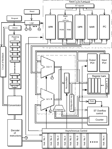
Instruction format: each instruction is divided into sections or fields, where each field is a group of bits that provide a part of the information required to determine the type of operation to be executed and the location of the data on which it will be executed. The instruction set avoids including micro-instructions that could seem attractive and of a big computing capacity, similar to high level sentences. The simplicity of the instruction set allows the control unit to be easily and quickly implemented in hardware. Because of their characteristics, all the instructions have the same length, this simplifies the design of the Self-Timed Centralized Control Unit (STCC) [Ortega, 05B]. The instructions included in the processor are of these types: data movements and transferring of register, displacements, arithmetical/logical instructions, control, jumps, and input/output instructions. Addressing modes used in this microprocessor are the following: direct, extended direct, implicit, addressing register, indirect register, and extended register. In the figure 1, you can see the overall diagram of the ST microprocessor, composed of the following main modules:
Page 378 ST micropipeline module: The ST micropipeline module is composed of (ACB) asynchronous control blocks. The micropipeline is connected in a ring, having an interruption of petition pulses controlled by the ST control unit [Ortega, 05B]. The configuration in ring allows to realize cycles repeated of requests and constant ideal recognitions for operations of recurrent calculating. Petition cycles are ruled by the ST control unit, the general reset and the external initialization of the main petition line of the processor. Figure 1: ST microprocessor architecture Page 379 Asynchronous control unit: The ST control unit is composed by an instruction decoder block, pass logic units and controlling of the petition and identification pulses to the processor modules (gathering/distributing elements). Arithmetical logical units: The processor has two arithmetical logical units; a) ALU 1, which executes 14 instructions of data transferring, of rotation-displacement, arithmetical and logical, which are executed in a direct way by the processor instruction group; b) ALU 2 that executes 6 instructions related to registers, data transferring, and comparing. Both logical units have 16 bits of word length. There is only one accumulator for both units; this allows the access of data from the output port in a direct way [Ortega, 05B]. Register bank: It is composed of 8 registers of 16 bits with direct access to the ALU 2, which are identified with the letters C, L, N, M. The L and N registers are for general purposes, here data or directions may be stored. The C register is for overflow configuration. The M register stores the quantity of cycles and indicates when an indefinite cycle shows up during the program processing. The X and Y registers have 16 bits and a direct access to the ALU 1 for logical and arithmetical operations. Fetch cycle hardware: The fetch cycle is composed of the following blocks:
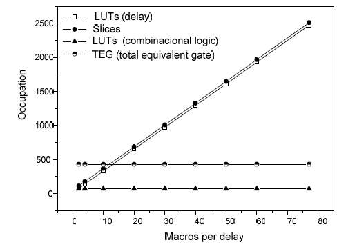
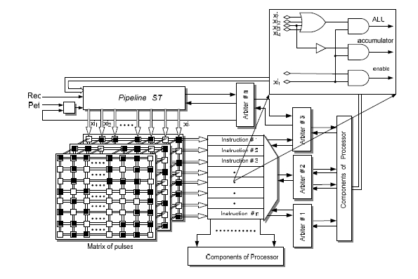
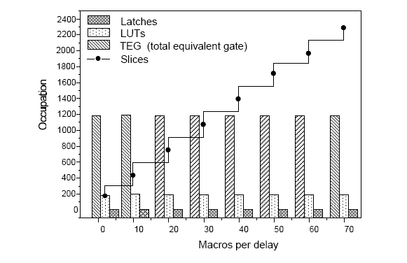
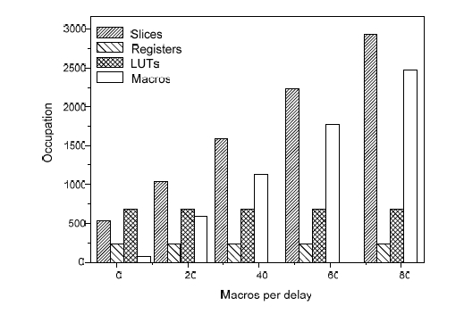
Input/output ports: Processor has two ports with 16 bits; one as an input and the second one as an output. The output port has a direct connection to the accumulator, so writing is a transferring of data between registers (accumulator to output port). The input port is a register that has a direct connection to the ALU 1. This configuration simplifies the execution of logical and arithmetical operations on the data coming from both ports. Setting and overflow control registers are designed to avoid that undefined calculation cycles showing up. Both circuits are complementary: the register configures the system of reset general or initiation of the system and the circuit of overflow executes the order [Ortega, 05B]. 3 ST Micropipeline in a ringThe ST micropipeline implemented in this processor has a ring configuration, its performance is determined by the number of asynchronous control blocks forming it. Specially, a ST with a ring is used in this work for development the fetch cycle. The STCC are based on these kinds of circuits. In the figure 2 the occupation is observed depending on the variation of macros of the ST micropipeline in ring used in this work. The occupation has the following characteristics: 33 ACBs, 32 delays and the feedback of the ST micropipeline in ring has one delay, which allows fitting the pulse of activation adequately. Page 380 If the amount of macros corresponding to each delay is changed as it is observed in the graph of the figure 2 (2 to 77), an increase in the number of slices from 13 to 50% of the total of these in a FPGA Virtex II, staying the total equivalent gates and that of LUTs. For what one concludes that to more number of macros there is a considerable increase in area. Figure 2: Occupation of the resources of the FPGA depending on the delay 4 Asynchronous control unitThe asynchronous control unit is formed of several combinational logical modules corresponding to each instruction and the circuits for the distribution of the activation signals. The control unit regulates data transferring and empowers the different elements of the processor in a sequential way each time that an instruction is executed in the microprocessor. The operation starts with a search cycle and continues with the execution of the instruction. The configuration of the unit of ST control is organized in such a way that with a pulse of request the asynchronous logic of control is activated, it convert a signal and establishes the sequence of activation of the components based on the instructions of the main program of the processor. The components are enabled in different periods and are activated sequentially, the control has an arrangement in matrix form which is in charge to send the pulses that activate to the components that form a part of the microinstruction, see figure 3. The "xi" activations coming from ST micropipeline are arranged in matrix, they activate an "AND-OR" plane in the asynchronous control unit, which determines the sequence and enable periods of the processor elements. To realize an instruction several signals of activation (xi) are needed, these are connected to the OR plane and this one produces a signal that activates to the AND plane in combination with control signals, as it is observed in the figure 3. Figure 3: Flow of the asynchronous control unit A delay is implemented with one macro, every macro occupies a slice. The figure 4 shows the resources used in the asynchronous unit of control with different numbers of macros, the unit of control with bigger delays increases the use of the slices and these are independent from the occupation of other components of the unit of control. The modification of the delays was realized to observe the behavior of the signal of control of the processor and to verify the stability of the signals with different delays. Page 382 Figure 4: Occupation in terms of macros for asynchronous control 5 Results of the interconnection during implementationTaking into account the distribution of the post-layout interconnection lines, resulting from the implementation to ST microprocessor with 2 macros per delay, the distribution of the lines is as follow:
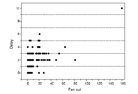
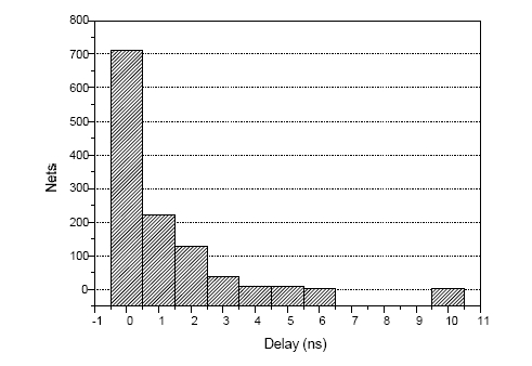
Results obtained from post-layout implementation of the fan-out distribution for ST processor are displayed in the figure 5. Reset line shows the maximum delay, 10 ns. 11 lines have delays between 2 and 4 ns, and the rest of lines show delays between 0 and 6 ns. Nets quantity in terms of delay in the ST microprocessor showed the distribution of the figure 6. Among 1120 nets, 63.5% of them have a delay less than 1 ns, 36% have a delay between 1 and 5 ns. Finally, only 2 nets showed delays of 6 and 10 ns respectively. Distribution of fan-out in ST microprocessor, with several macros per delay, shows a similar behaviour [Ortega, 05B]. Proving this way that connectivity is maintained independently of the increase of macro per delay in the ST micropipeline of the control unit. Figure 5: Fan-out in terms of delay for ST microprocessor Figure 6: Quantity of nets in terms of delay Page 384 6 Occupation of the resources in the FPGAIn order to implement Self-Timed circuits, it is important to take into account the resources of the FPGAs. In a ST circuit, data transferring control uses a big quantity of logical ports, contributing to the increase of final occupation. In the graph of the figure 7, there is an example of the above mentioned, where the occupation resources in the FPGA are showed for the ST microprocessor with different quantity of macros used for implementation of delay [Ortega, 05]. We can see that increase of slices is proportional to macros increase. We have to point out that, registers and LUTs remain constant, so the increase of the resources is mainly attributed to the macros increase. The percentage of occupation of the microprocessor with 2 macros is 18% of slices, compared to the 77 macros processor; i.e. the last one is more or less 5 times bigger than ST microprocessor with 2 macros per delay. In the figure 8, we can see the distribution of the resources used by the different modules which form the ST microprocessor. As we can see, memory module has the highest level of occupation, with 6.5% of (TEG) Total Equivalent Gate count for design available in FPGA. Arithmetical blocks are the 2 modules with higher occupation, 0.29% for ALU 1 and 0.14% for ALU 2. ST control module is the fourth biggest one, with an occupation of 0.11% of the TEG in the FPGA. These results correspond to microprocessor with 2 macros per delay. Figure 7: Occupation in terms of macros per delay for ST microprocessor Page 385 Figure 8: Occupation of the components of the ST microprocessor with 2 macros per delay 7 ConclusionsIn this article, we have introduced the results of implementation of ST AMCC processor, from these results we can conclude as follow: Implementation of ST control circuits or blocks in Xilinx FPGA devices shows that these circuits or blocks can be used to make a quick prototype. Implementing delaying macros in the FPGA editor, we can obtain a determined fixed delay to make equal processing times to computing blocks and to establish a correct synchronization of the data flow in the microprocessor control. The ST microprocessor developed in this work shows an execution of 9.6 MIPS, for detail of estimate the microprocessors execution [Ortega, 05B] And include inherently the stoppable clock feature; i.e., circuit is stopped if it is not required (minimal dynamic consumption). Acknowledgements To the University of Guadalajara by the economic support that offered for to present this work. Page 386 References[Beerel, 02] Beerel P.A., "Asynchronous circuits: An Increasingly Practical Design Solution", Proceedings of the International Symposium on Quality Electronic Design (ISQED02) 0-7695-1561-4/02 IEEE 2002. [Berkel, 96] Berkel K. V. and Bink. A., "Single-track handshaking signaling with application to micropipelines and handshake circuits", In Proc. International Symposium on Advanced Research in Asynchronous Circuits and Systems, pages 122-133. IEEE Computer Society Press, March 1996. [Brunvand, 99] Brunvand E., Nowick S., Yun K., "Practical advances in asynchronous design and in asynchronous/synchronous interfaces", Proc. 36th Design Automation Conference, pp. 104-109, 21-25 June 1999. [Furber, 96] Furber B. and Liu J., "Dynamic logic in four-phase micropipelines", Advanced Research in Asynchronous Circuits and Systems, 1996. Proceedings, Second International Symposium on, pp. 11 - 16, 18-21 March 1996. [Ortega, 05] Ortega S., Raygoza J.J., Boemo E., "Diseño e implementación en FPGAs de elementos de control pipeline con protocolo de sincronización Self-Timed", V Jornadas de Computación Reconfigurable y Aplicaciones (JCRA'2005), ISBN:84-9732-439-0, pp: 375-380, Granada, España, Septiembre 2005. [Ortega, 05B] Ortega S. "Diseño de Circuitos con Protocolos de Sincronización ST en Dispositivos Programables FPGAs", Tesis presentada en la EPS de la U A M, Noviembre 2005. [Theodoropoulos, 95] Theodoropoulos G., "Strategies for the modelling and simulation of asynchronous computer architectures", Thesis submitted to the University of Manchester for the degree of PHD, Faculty of Science and Engineering, 1995. Page 387 |
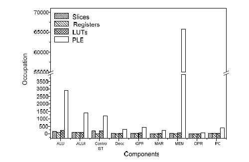
|||||||||||||||||