Protecting Devices by Active Coating
(A method to build a signature based microsafe)
Dr. Reinhard Posch
Technische Universität GRAZ, AUSTRIA
Reinhard.Posch@iaik.tu-graz.ac.at
Abstract: The presented paper demonstrates a method to embed
a unique signature into a coating material used in a smart card or in the
covering material of some other secure hardware device. The method bases
on the impossibility of exactly reproducing a specific piece of plastic
or other material used to cover the secure hardware. By using a very inhomogeneous
materials or mixtures of conductors and insulators such a cover is made
unique by the method of production. This inhomogeneous piece and the non-reproducible
and random properties are incorporated into an electronic signature which
is checked whenever needed. Assuming that the surface is covered totally
with an "active coating material" it is impossible to partially
penetrate or destroy the coating without destroying the signature. Unpenetrable
hardware is an inevitable element in nearly all secure designs and with
the promotion of digital signatures such unpenetrable hardware becomes
even more important. The result gained with the presented work is the possibility
to make a hardware unique depending on randomness, and to assure that penetration
is not only detected but also features logical destruction of the secure
hardware [PAT96]. Implementing such penetration sensors
with memory enhances the security to a large extent, and since the destruction
upon perceived penetration is logical there is no possible false alarm.
1 Introduction
This document assumes a computing device whereof a distinct part contains
relevant secure information that has to be guarded by special means. It
further assumes that this distinct security module SM is well separated
from the rest of the hardware so that it is possible to take design measures
which allow detection, monitoring, prevention and
reaction on an external
attack to the module. The paper concentrates on features of design and
construction of such an SM. Security of peripherals as well as modules
outside to SM are not addressed.
The overall structure may be seen as shown in figure 1. Special attention
is paid to the security module SM and to methods of how to implement
security guards G. The first observation which can be made is that
the task of secure designing is smaller when the diameter of the security
module gets smaller. In practice this means that security keys and application
of security keys (encryption, decryption and signing) will define the size
of the security module in many cases. This observation is based on a second
assumption which says that security design primarily concentrates on the
controlled use of the security module and on the leakage of information
from this module but does not widely address aspects of theft and destruction
of the module as long as there can be assured that stolen modules or broken
modules do not deliver secrets. This assumption is consistent with the
fact that data as bits do not have a value but only data as content define
a specific value.
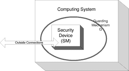
Figure 1: The setup of the discussed computing environment.
A second aspect is governed by the question "At what times should
protection be in place?" The answer seems obvious: protection should
be effective any time when there is valid and usable information within
the module. Still, we may distinguish at least three situations:
- Cold: the security module is not powered at all. This
is the case at least during long term storage usually before the first
use. For
some systems like smart cards this situation also occurs between
regular use with information in the module. This seems to be the most critical
situation as the security features are passive in this case.
- Warm: the security module is minimum powered. Only the
main security features are turned on and the security guard G is
actively protecting part or all of the module.
- Hot: the security module is operating and powered with
the security guard G operating as well.
It is obvious that the amount of security does not depend on the status
of a device, but mostly on the security information a possible attack could
reveal. But the effort of guarding mechanisms could be totally different
in different situations.
Typically the largest amount of information present and eligible for
an information guard will exist in a hot device. The status warm
only exists in special devices at all where a buffering of power is possible
to maintain vital functions. With such devices a minimum power usually
is applied during life time of the device. Even if this seems to be the
most favorable condition for guarding when some activity may be assumed,
at any time one has also to consider devices where power is completely
off during long phases, and possible attacks happening during this time.
This cold device situation has to be faced with all smart cards.
The fact arises from standards [ISO89] which de facto ask for a single
component solution giving no place for power supply for buffering. Since
smart cards are discussed in the context of digital signatures, the cold
situation seems to be the most important one.
In practice, we observe that the security systems considered for wide
applications suffer various security problems.
2 The Model
As seen from figure 1 we concentrate on the core of a system which we
assume to be well separated.
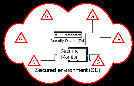
Figure 2: Security device with guards.
Around the module SM security guards G, i.e. sensors,
are allocated to register different types of abnormal conditions. These
sensors report to a security monitor. A set of conditions as sensed by
the various Gs is defined as valid operating conditions OC.
Any violation of OC is assumed to be seized, and an according security
response SR is assumed to take place after a predefined reaction
time Tr.
This model describes a closed shape S of many dimensions enclosing
some device SM. An attack can be viewed as trace propagating at
some speed v towards the center where the module SM is assumed.
As long as the total time Tr from recognition to measures
taken at any moment is less than the minimum distance from the entry point
through guarded shape S to the module SM divided by the maximum
possible speed, the situation is seen as safe.
With the different possible states of a module SM in mind it
is important to look at the situation as a dynamic process. Furthermore
it is useful to add the dimension of cost, as done later on, in this context.
A successful attack is an attack leaking or altering information
of the module SM without the defined countermeasures being taken
in due time. Some of the possible scenarios of an attack are pointed at
below. This is done to demonstrate the large diversity of possible attacks
and thus the complexity of the matter. Basically there are two categories
of an attack:
- Non destructive attacks: in this case the module SM is
observed from outside and gathered information is misused. The module SM
stays operable, and in the optimum case the presence of an
attack cannot
be seen on the module after the end of the attack. Attacks destroying some
of the guarding mechanisms are included in this attack intentionally.
- Destructive attack: such attacks will destroy the module, but
some or all of the information which was designed to be secret to SM
will be compromised. This attack is much less severe and sometimes is assumed
to be overcome by logically unique devices. This method of unique devices
by only using unique key information is a common technique in the field
of smart cards. For reasons of consistency an attack which gathers all
or most of the secret information in an way that a non-distinguishable
device SM* is generated and replaced has to be classified as a possible
non-destructive attack. This is due to the fact that this discussion concentrates
on information.
Generally it would be possible to distinguish between attacks addressed
towards hardware and those addressed towards software. This distinction
is not extremely useful in practice, as most attacks combine both domains.
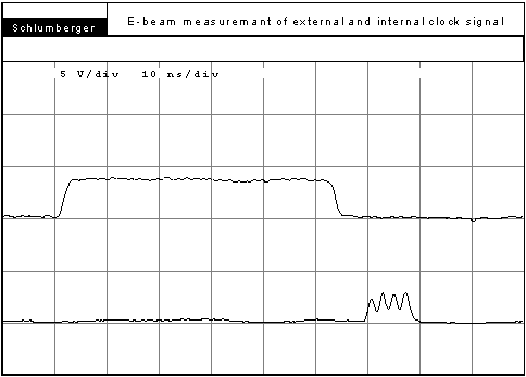
Figure 3: E-beam analysis of a 450MHz digital signal.
From the technical point of view the discussion presented focuses on
the following categories:
- Observation of primary and secondary effects: this includes
data communicated, sequences, crosstalk, radiation, etc.
- Modification of operating conditions with the goal to change the
internal function: this category includes temperature, power supplied,
frequency, radiation, light, etc.
- Measuring and injection of signals internal to circuits: in
the context of smart cards this would include probing with conventional
methods, electronic beams, focused ion beams, etc.
Even if a special attack like injecting and probing of signals at extreme
temperatures would fall into several categories, it seems to be useful
to use such categories since measures to be taken are quite different along
with the various categories.
To give an idea what the state of the art makes possible in special
cases, figure 3 shows an E-beam analysis of high frequency signals. In
this special example a high frequency signal was analyzed. The result of
this example shows that signals even at extremely high frequencies can
be intercepted if no specific measures of protection are employed.
Since it may be assumed that expensive attacks are only performed when
the revenue from the attack is adequate, it is essential to draw a limit
V for a special module SM , reflecting the amount of money
this module is able to protect. This observation is quite obvious to reflect
in monetary systems, but becomes a lot more complicated in medical systems
or in systems of personal safety or national security.
3 The Formulation of the Problem
As we are considering device security against compromise by hardware
analysis, we can formulate the specific security problem the following
way:
Csec Cost of the security enhancing technology.
Canalyse Cost of a successful analysis.
Vp Value to be protected by the respective security
technology.
- Security is viewed as manageable in business terms if the condition
Csec <<Vp is satisfied.
- A system is viewed as secure in the special context if the condition
Canalyse >>Vp is satisfied, or in some
cases Canalyse >>
![]() (Vp),
where (Vp),
where ![]() (Vp) is the total of all values secured with
the respective technology, is satisfied. (Vp) is the total of all values secured with
the respective technology, is satisfied.
The arising problem in all these cases is that the condition resulting
from the above Canalyse >>> Csec
is generally quite complicated to match when looking at hardware components.
The situation becomes even more complicated if the values secured with
the technology cannot easily be measured in terms of money. In this case
a value Vp could be substituted.
4 A Method to Inhibit Physical Access
Having stated the problem of securing hardware, this chapter concentrates
on a method to implement guards for electronic devices. The security target
is to inhibit secret information from leaving the security boundaries or
being altered. In this context, securing a hardware is assumed to be successful
if relevant information can not be altered or extracted by an aggressor.
The presented method targets primarily VLSI chips like those used within
smart cards. However, the general principle can be applied to other electronic
devices containing at least a processor or using a processor to perform
the guarding operation in a similar way.
Smart cards are for the time being quite in danger to be exposed to
"microprobing" and similar methods. To prevent for this regulations
like the FIPS 140 [FIPS94] demand for special covering
for such devices in order to inhibit etching a cover and getting access
to an operable device exposed for analysis.
The method discussed with this paper does not prevent analysis as such,
but uses a coating mechanism that can be classified as a sensor with memory
and storage for key information. Tampering with this type of coating leads
to a change in the key information and thus tampering destroys such key
information. This key information is used to decrypt [SCHN96]
critical information to yield the useful information. Such decryption can
only be performed in a hot state as classified above. This leads
to the situation that the overall security is the security implemented
in the hot state.
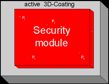
- Security module (red) (SD)
- Secure coating (grey) (M)
- Security guards (Pi)
Figure 4: An encapsulated secure unit.
Figure 4 shows a general three-dimensional model of a coated security
device. This security device denoted as SD is shown with the coating
M and the security guards Pi on the surface of
the unit SD. The basic assumption is that by using appropriate mixtures
or materials, the coating shown in grey may be implement in a way resulting
in random electrical properties like resistance and capacitance. A geometrically
identical duplicate will this way have different electrical properties.
Removal and re-application of the coating similarly is assumed to change
electrical properties of the coating.
This unique coating characterizes the specific device. And from this
characterization a device signature ST is derived.
4.1 Components of "Active Coating"
- Be (SD) a unit like a smart card to be secured, then the measure
shall detect manipulation both during operation and during off-powered
storage, and information shall not leak in any situation by design.
- Be (M) some coating to secure SD. Such coating is assumed
to be of a material that has an electrically measurable property (like
resistance or capacitance), but is highly inhomogeneous and irreproducible.
- (Pi) are spots on the surface that can apply some
signal or measure the value of the property.
4.2 The Pi Spot
The Pi spots are designed to apply and measure electrical properties.
In case of a smart card the spots Pi are areas somewhere
on the chip surface that look like pads but are as small as technology
allows. This way these spots contact to the inhomogeneous coating material.
The I/O pads and power pads themselves are assumed to be covered by an
insulating material after ponding. In the simplest case, a Pi may
serve as output switching either some stable reference Vref or VSS
to the Pi spot, or as input sensing the voltage via an
analog switch by usage of an analog busline connected to an A/D converter.
This gives the possibility to select an arbitrary spot for sensing out
of the available spots. This situation is shown in figure 5a.
4.3 Signing the chip coating
Using different spots with different output values mi
and combining the respective input values si using an
appropriate function ST = f(mi ,si), coverage
over the surface shall be achieved so that tampering at any spot on the
surface will at least change one of the relevant inputs significantly.
As f() can be chosen as a hash function, selective tamper is impossible.
If needed, temperature may be compensated by setting different temperature
intervals. This procedure assumes that the sensed values si
are not too close to a value that changes with a small variation in
a way that significant digits are changed after the rightmost digits are
truncated. If this situation happens this value is discarded, and by rearranging
input and output spots a more stable situation is found. As the value ST
is kept within the device all the time, it can be used asymmetric key both
for encryption during setup and decryption before use of relevant secret
information and code pieces.
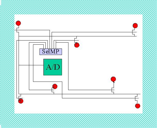
Figure 5a: Example of chip with A/D and Pi
spots.
5 How to Apply the Signature of the Coating
If temperature intervals are not necessary, the ST value of the
equation above may be used as a key STNorm. In the case
of different intervals with different temperatures D STj
denominates the difference between the signature STNorm
(e.g. at 25° C) and the signature for the temperature interval j.
The ![]() STj values are stored along with the output and
input locations. In the course of initialization, ST is used to
encrypt all relevant secret information. It can also be used to sign the
program code if necessary. As only differences are stored, it is assumed
that theses values do not deliver information on STNorm. STj values are stored along with the output and
input locations. In the course of initialization, ST is used to
encrypt all relevant secret information. It can also be used to sign the
program code if necessary. As only differences are stored, it is assumed
that theses values do not deliver information on STNorm.
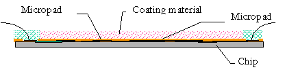
Figure 5b: Sectional view of 5a.
Step I: Determine STj thus STNorm=STj-![]() STj.
STj.
Step II: The security relevant information is decrypted using STNorm.
Due to inhomogeneous properties of the coating material the coating
is assumed not to be reproducible. As ![]() STj and STNorm
are calculated during initialization it is assumed that in a proper design
this information never leaves the unit SD. STj and STNorm
are calculated during initialization it is assumed that in a proper design
this information never leaves the unit SD.
6 Scenario of an Attack
As a consequence of available design methods [WES92]
the most promising attack still is to tap on signals of a given smart card
design. In many cases this means that locations of signals on the surface
are identified and seized with probes inserted. At the same time such locations
can be used to insert signal so that the operation of the smart card is
influenced in a way that information is gained by the attacker as much
as possible.
- In the presented situation the coating material is not a simple insulator.
Thus, any contact between the probe and the coating material will influence
the signals probed. Assuming that the resistive and capacitive properties
are adequate, the influence on the signals on the chip will be such that
the results are heavily distorted and the general behavior of the smart
card is changed.
- Any contact between the probe and the coating material will strongly
influence the values probed by the signature mechanism of the coating.
This will result in a situation where the signature is invalid and no information
is acquired. This basically has the result that the area where the coating
material has to be removed to make probing possible is necessarily relatively
large so that contact between probes and coating can be avoided (see also
figure 6).
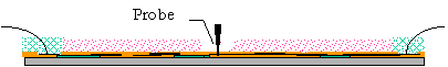
Figure 6: Scenario of a probing attack.
The figure above shows an attack of a chip guarded by active coating.
In the general case it will take some effort to find a spot on the chip
exactly, since non-transparent materials are assumed. The fact is that
the hole to dig into the coating material will be substantially larger
that in the case of transparent material.
If the Pi spots are dense enough on the surface of
the chip, it may be assumed that even partially destroying the coating
will result in at least one value relevant to the signature being changed;
thus the secret information can no more be decrypted. Removing larger parts
of the coating will have at least as severe effects, and thus the coating
is to be assumed secure by having an equivalent of a fraud-resistant memory.
Similarly to the probing attack, the method of active coating may be
structured in a way that many aspects of a differential fault analysis
are covered [DFA96]. This aspect is not dealt with
in detail, but just some basic related thoughts are presented. The method
strongly bases on the fact that only correctly retrieved signatures from
the coating allow continuation. This is basically achieved by the potential
of encrypting some of the consequently executed code. This way any fault
in retrieving or applying the signature of the coating may be assumed to
result in a complete faulty operation. Neither the result of the retrieved
signature itself nor the result of the encrypted data when applying the
signature as a key are ever seen by the outside, but stay totally internal
to the device.
It is, however, obvious that all the measures necessary to inhibit DFA
in consequent operations have to be taken. Repeated application of the
signing mechanism can be one component in this direction. In this context
it seems to be useful to take advantage of the fact that keeping parts
of the results of the coating signature in the encrypted part of the device
is not an extra security risk.
7 An Active Coating Demonstration Module
To demonstrate the effect of active coating, a demonstration module
has been built. This module which is shown in the figure below uses a very
small number of sensing points. It simulates only a part of a surface of
a security device.
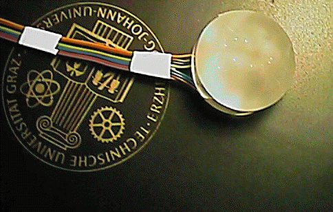
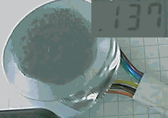
Figure 7: A coating demonstrator.
The security device is simulated by a block of resin where the micropads
are the tips of thin wires. In figure 7, these micropads are pointed at
with red arrows. The surface shown in figure 7 would reflect the surface
of a chip where the coating should reside on. For the demonstrator the
VLSI device has been substituted by a cable leading to the computer.
Coating was actually provided by using graphite and paint as an inhomogeneous
material. To demonstrate the effect, the first layer of the coating material
which ultimately has to have a three dimensional property is shown in figure
8. There, only the resistive property is demonstrated.
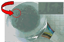
A simple violation of the device integrity is simulated by touching
the coating with a metallic probe. The result can be seen between the micropads
S and T. The change of the resistive property due to the integrity violation
was over 10% in this case.
Figure 8: Tampering with an active coating device.
In this simple case only 8 micropads were included. The position where
tampering has taken place is shown in the circle in figure 8 b). In the
practical case, the number of micropads would have to result from external
observability of the coating. It is assumed that two to four bits are taken
from each micropad, thus resulting in a realistic number of 30 to 80 micropads
for a single chip device.
8 Handling Temperature and Environment
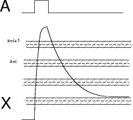
Figure 9 shows the situation of a single actuator A and the function
of the shield (ground). While in practice there will be many more, this
model is introduced to concentrate on the handling of environmental conditions
and aging. Besides accuracy of sensing the coating properties, there are
several facts to consider as the keys derived from the sensing process
need to be unique and, as they are not stored anywhere, well reproducible.
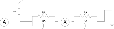
Figure 9: The sensor model.
We concentrate on two types:
- The aging effects.
These effects will allow sensing values to migrate slowly from an original
value to an asymptotic value. I this case the main assumption is that a
module, protected with active coating is not out of operation for excessive
periods of time. Under this condition a feedback mechanism can be introduced
so as to compensate for such effects.
- Environmental effects.
Such effects temporarily influence the key retrieval. Temperature and
humidity are obvious examples.
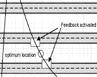
Figure 10: The
critical areas.
As shown in figure 10, the described situation results in a split into
sense values that may be used as they are, and into sense values that need
post processing and feedback. This feedback is used to bring the sense
values back into the optimum position. Feedback is done by changing the
pulse width on the actuator A. As only discrete values of the sensed value
X are used, and as the change in A is only used to modify the unused part
of the sense value, this is not assumed to influence security.
Temperature is still a further problem. This parameter may influence
in a wider range. For that reason the system assumes that a temperature
sensor is included. As a result of the ambient temperature, a bias to the
actuator value A is calculated or retrieved from a table. These measures
are used to ensure maximum operability of the system.
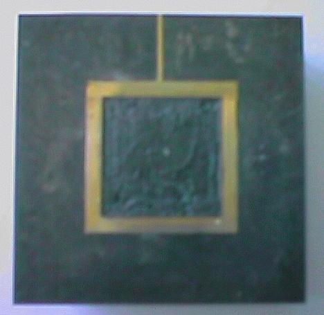
Figure 11: A Sample chip with coating.
To gather sample data and to verify the basic assumptions a sample chip
has been coated with a mixture of resin silver and graphite resulting in
a fairly inhomogeneous
cover material. Both resistive and capacitive effects
have been evaluated using this sample chip. To judge on stability the sensing
points have been made available at pins on the outside.
9 Further Applications and Conclusion
Independent from the above mentioned, active coating can also be used
for further applications associated with the application of encapsulating
a security device.
- A first application is the substitution of test fuses usually built
into a smart card device to distinguish between the initial test of a device
and the operation of the device. If it is assured that even during test
the unique information of the coating is not delivered upon a certain procedure,
the method of active coating can be used to implement fuses. The simplest
way is to define the fuse to be blown if the decryption of a certain value
matches a given location. If this procedure is implemented properly, this
results in the perfect fuse. Even if logically reconnected by e.g. destroying
the coating or partially changing the coating signature, there is no danger
as all information is logically destroyed with this effect. Thereafter
the device could even be reused and reinitialized from the technical point
of view. From a security and systematic point of view this should not take
place except when the change of the coating properties is performed in
a secure environment in order to reinitialize the device.
- A further application of the coating could be the secure transport
of uninitialized devices. This is a problem with large quantities of devices.
Secure coating is not an easy problem. However, it is vital for many
applications and most present designs of smart cards have to be classified
as penetrable with appropriate means. Even with special chemicals used
for coating it is very complicated to install coating on chips that meet
the demand that tamper is also damaging the chip's function and that it
can thus be made sure that secret information in not possibly acquired,
active coating may contribute to this problem in a consistent way. Making
cryptographically sure that any change in the coating is closing down the
access to information promises to serve the purpose of building an effective
microsafe in many contexts like electronic purses and smart cards for digital
signatures. This
method of a self-signing microsafe can also be designed
to defeat many aspects of a differential fault analysis attack when applied
properly.
References
[FIPS94] NIST; Processing Standards Publication
140-1 1994 - SECURITY REQUIREMENTS FOR CRYPTOGRAPHIC MODULES, NIST, 1994.
[ISO89] ISO; ISO/IEC 7816-3: Identification cards
- Integrated circuit(s) cards with contacts - Part 3: Electronic signals
and transmission protocols, ISO, 1989.
[SCHN96] Bruce Schneier; Applied Cryptography,
John Wiley & Sons Press, 2nd edition, New York 1996.
[WES92] Neil H.E. Weste, Kamran Eshraghian; Principles
of VLSI Design, Addison-Wesley, Reading 1992.
[PAT96] R. Posch; Verfahren und Anordnung zum Schutz
von elektronischen Recheneinheiten, insbesondere Chipkarten, Patentanmeldung
Wien 1996.
[DFA96] Ross Anderson, Markus Kuhn; Tamper Resistance
- a Cautionary Note, Proceedings of the 2nd Workshop On Electronic Commerce,
Oakland, California, November 18-20, 1996. (to appear)
|