| Submission Procedure |
Testing a High-Speed Data Path The Design of the RSAb Crypto Chip(Graz University of Technology, Austria wmayer@ iaik.tu-graz.ac.at) (Graz University of Technology, Austria kposch@iaik.tu-graz.ac.at) (Graz University of Technology, Austria rposch@iaik.tu-graz.ac.at) (Graz University of Technology, Austria vschindl@iaik.tu-graz.ac.at) Abstract: High speed devices for public key cryptography
are of emerging interest. For this reason, the This work has been sponsored as part of the project Nr. P9384PHY "Sichere Kommunikation bei hohen Geschwindigkeiten" by the Austrian Science Foundation. Keywords: high speed multipliers, hardware algorithms, design for testability, public key cryptography 1 Introduction
Simulating a CMOS VLSI design and testing the prototype of a newly
designed chip is a sophisticated and time consuming task. This is in
particular true in the special case of the RSA - The modulo multiplier is built in modified domino logic [Weste et al 1993], which results in smaller area and higher speed, but requires a very careful design process. Page 728 - The necessity for handling very large integers for a secure RSA implementation causes a width of the MM data path of about 700 bits. Designing CMOS circuits of this size leads to specific problems not present when designing much smaller systems. Therefore, it is quite advisable to spend very much effort on simulating the chip's function, and to provide built-in testing features. Furthermore, standalone testing of the MM data path without control logic driving it would be a preferable strategy. We will concentrate on the last item. Real stand-alone testing of the MM data path in a separate package results in feeding its control signals directly via the chip's pads. At this point, a problem arises: The maximum clock rate allowed by the pads is lower than the clock rate we would need at the MM data path to reach the desired processing speed by a factor of about 5. It makes no sense (and even might be impossible for dynamic logic) to test the MM data path at a much lower speed than it was designed for. Therefore we cannot avoid adding some kind of control logic between the pads and the MM data path. Test results should not be influenced by that control structure. It should not cause any changes to the layout of the MM data path, and it must be of very high reliability. Both requirements call for an "as simple as possible" control structure. The key for finding such a minimum version of the control structure is to analyze the control signal flow, which allows for reducing redundancy, and even leads to the use of a modified version of the original modulo multiplication algorithm for optimizing control signal flow. In this paper, we will take a closer look at the modulo multiplication algorithm (which is the heart of the RSA implementation), as well as at the MM data path designed for performing this operation efficiently. After analyzing the control signal flow, enough information is available to introduce a simple mechanism for compensating the clock rate difference without loss of overall performance. Finally, we will show an outline of a possible hardware implementation. 2 The FastMM Algorithm
The RSA algorithm [Rivest et al 1978] performs both, encryption and decryption, by calculating 
With the RSA  which is much easier to compute than the exact modulo multiplication  Page 729 as it avoids division and uses multiplication only like the Montgomery approach [Montgomery 1985]. We will refer to y as relaxed residuum, since it is possibly not fully reduced. The efficiency of FastMM is based on a fast and good approximation Q of the quotient  Q is calculated as follows:  k is the length of the modulus N in bits. For convenience, we introduce  Note that both, NegN as well as N1 can be precomputed. Now, FastMM
can be represented using the following symbolic instructions  In [Posch et al 1990] it is shown that the results of continued relaxed modulo multiplications never exceed the limit given by e. Therefore, only after the last multiplication a final modulus reduction might be necessary. Obviously, this reduction step does not decrease throughput, compared to the hundreds of modulo multiplications which are to be performed for getting the relaxed result. This final modulus reduction can be done by adding NegN to the result. Note that NegN and the possibility to perform an addition are needed by the FastMM algorithm, anyway. Therefore, the final modulus reduction requires no additional hardware effort or constants. 3 The MM Data Path
3.1 The Structure of the MM Data Path
The design of the MM data path, shown in [Figure 1], meets the special requirements of the FastMM algorithm. It consists of several main registers with length 696 bits (IO, Cph, Mkd, NegN, N1, Low, High), an APAP-structure [Lippitsch et al 1991] (described in [Section 3.2]) and a few auxiliary registers of length eight bits. Adder-1 and Adder-2 are needed for converting the redundant number representation used by register High and the APAP-adder - into binary numbers. Adder-3 performs the addition of multiplication step (C). The purpose of the transmission gates as well as the overall function of the MM Page 730 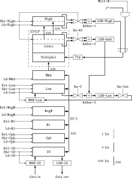
Page 731 data path will become clear in [Section 3.3]. We will use the main registers in the following way: The IO register is needed for input/ouput operations, Cph (for cipher text) is commonly used for storing the last result while the next modulo multiplication is running. NegN and N1 hold the corresponding constants mentioned in [Section 2], Mkd must contain the actual multiplicand. Low receives the lower part of the result of a multiplication in binary number representation, while High gets the higher part in redundant number representation. The MM data path requires quite many control signals, denoted as a control word. We present a complete list of the control signals which shows the actions in each clock cycle if the corresponding signal is active: Evl-X: Write value of register X to the 696 bit bus, where X can be one of the following: IO, Cph, NegN, N1, Low. Ld-Y: Load register Y with the value of the 696 bit bus, where Y can be one of the following: IO, Cph, NegN, N1, Low, Mkd. Ld-High: Load register High with the current value of the APAP-adder, then clear the APAP-adder. Shr-High: Enable storing the least significant byte of register High to LSB-High, then shift High to the right by one byte. Shr-Low: Shift Low to the right by one byte, including MSB-Low. Shr-IO: Shift IO to the right by one byte including MSB-IO, thus loading a new byte from outside via MSB-IO. LSB-IO buffers the least significant byte of IO and provides it for output. Shr-Cph: Shift right Cph by one bit. En-AC: Enable storing the least significant byte of the APAP-adder to LSB-Add during operation (A) resp. (C) of FastMM. En-C: Enable storing the least significant byte of register Low to LSB-Low during operation (C) of FastMM. En-Cut: Cut off the bit stream on changing from high to low. 3.2 The APAP-Structure
The APAP (As Parallel As Possible)-structure represents a mixture of a serial/parallel multiplier and a full parallel Wallace tree multiplier [Wallace 1964]. This approach has been chosen because for long integer arithmetic conventional serial/parallel multipliers would be far too slow, whereas a full Wallace tree multiplier cannot be implemented on reasonable chip area with current technology. The degree of parallelism (i.e., the number p of new partial products that can be processed each cycle) may vary between certain boundaries, which allows for scaling the APAP design. To avoid carry delays, redundant number representation is used. For our purpose, we hide these implementation details, since we are only interested in the overall understanding of control signal handling. Therefore, we consider the APAP-structure together with Adder-2, as well as High together with Adder-1 to be "black boxes", thus hiding the internal function of the APAP-adder and the redundant number representation. (However, for Page 732 understanding the timing of the control signal sequence, the number of
cycles consumed by the APAP-adder and Adder-1 resp. Adder-2 would
have to be known.) Multiplication can now simply be described as a
serial/parallel multiplication, where p bits of the multiplier are
processed each cycle. For the RSA The following example [Figure 2] provides such a pure behavioural description 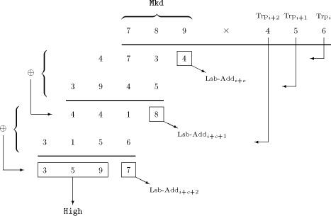
of the multiplication procedure. It uses decimal digits instead of
bytes, showing the principle of calculating the product of the
multiplicand 789 and the multiplier 456. The APAP-adder gets the first partial product (PP) by multiplying the multiplicand (held in Mkd) with the least significant digit of the multiplier. Note that the least significant digit of this PP represents the least significant digit of the the final result and can be loaded into Lsb-Add. Therefore, this PP is shifted to the right by one digit, being aligned for the addition with the PP of the next multiplication cycle as well. The least significant digit of the result of that addition represents the next digit of the result, and so forth. After the multiplicand has been multiplied with the most significant digit of the multiplier, the APAP-adder contains the higher part of the result, which can be loaded into High. Note that the APAP-adder always shifts its content to the right by one byte Page 733 each cycle, while Low resp. High can be forced by the corresponding control signals to do so. It is important to understand that the MM data path is able to perform these actions in parallel: For example, while the APAP-multiplier is fed from High via Trp with a sequence of bytes to multiply, former multiplication results may be shiftet into register Low. There are concurrent data streams, and their flow is controlled by a few control signals. 3.3 Performing a Modulo Multiplication with the MM Data Path
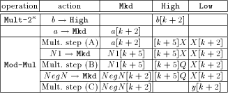
Table 1 shows the overall scheme of the modulo multiplication with the
MM data path. Once registers NegN and N1 are loaded with the
corresponding constants, the multiplier b must get into
High. Figure 1 shows that this can only be done by loading it into
Mkd first, followed by a multiplication by one. We will call this
operation Mult- After loading Mkd with the multiplicand a, we can start with operation Mod-Mul, the modulo multiplication using the FastMM algorithm. Figure 3 - which shows the control signal waveforms of a 664-bit modulo multiplication simulation - can now be understood: We start multiplication step (A) with setting high Shr-High to feed the APAP- structure with the multiplier byte by byte. En-AC, En-Cut and Shr-Low are also set to high for shifting the lower part of the intermediate result into Low: it will be needed in step (C). When the higher part of the result is ready, it is loaded into High by activating Ld-High. At the same time, N1 can be loaded into Mkd, starting multiplication step (B). This step is similar to step (A) except that shifting the result into Low is omitted. Step (C) starts with loading NegN into Mkd and is equal to step (A), but additionally sets En-C to high, thus adding the lower part of the multiplication result with the previous content of Low. After this procedure, the final result can be fetched from Low. Page 734 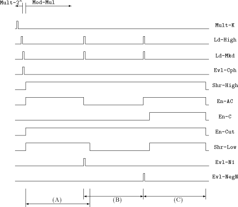  and
Mod-Mul and
Mod-Mul3.4 Observations about the Control Words
We note that the two operations Mult- With respect to [Section 5] it is useful to consider an atomic sequence as a sequence of stable sections, where the number of the stable sections is called the Page 735 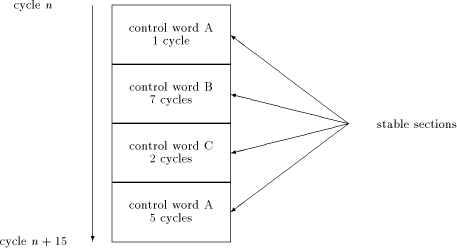 depth of the atomic sequence. Figure 4 shows an atomic sequence of a length of 15 cycles and depth 4. 4 A Modification of the FastMM Algorithm: FastMM*
A closer look at the FastMM algorithm shows that truncation of
intermediate results is necessary. For reasons of regularity it would
be easier to implement truncation only at multiples of i bits rather
than at arbitrary positions. With FastMM, values would generally be
cut off at positions To facilitate implementation, a
solution of this problem is given by a method called
preshifting. With this method, constants NegN and N1 as well as a and
b are preshifted to the left by certain values. Loading the multiplier
into High is done by using a It is needless to mention that these additional procedures make the handling of the control signals more complicated. Therefore, the lengths of stable sections within the atomic sequence of operation Mod-Mul are shortened, increasing the depth of the atomic sequence - this is disadvantageous, as we will see in [Section 5]. For that reason, we would prefer an algorithm which avoids these difficulties. Page 736 The obvious goal in algorithm design is to minimize depth for a given algorithm by control word rearranging. A solution is given by a modified version of FastMM, called FastMM*. FastMM* consists of the following steps: 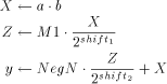 The basic idea is to apply shifts only to constants which can be
performed in advance. This algorithm has the same structure as
FastMM, but uses a different constant M1 instead of N1. Preshifting
will not be necessary because 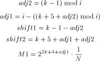 k is the length of the modulus N in bits. A further benefit of FastMM* is that it allows optimization in terms of
the possibility to change more control signals at the same time
(i.e., a higher degree of parallelism) than with FastMM. This results
in a significant reduction of the depth of the atomic sequence
associated with Mod-Mul. Additionally, for FastMM* 5 Managing the Clock Rate Difference Using a FIFO
In this section, a method for compensating the difference between the maximum clock rate allowed by the pads and the clock rate of the MM data path is presented. First, data flow at the control signal interface will be reduced. This can easily be done because the MM data path doesn't need to be fed with one control word each cycle if we use stable sections instead. Each stable section is described by the corresponding control word and the numer of cycles it is "stable" [see figure 4]. The control structure between the pads and the MM data path now consists of a buffer for the control word, and a down counter to decide when to fetch the control word of the next stable section. That would be sufficient if each stable section consisted of enough cycles, ensuring that continuous fetching of control words never exceeds the maximum clock rate allowed by the pads. Page 737 Unfortunately, there are a lot of stable sections consisting only of a few cycles. Therefore, a mechanism has to be added which feeds internally generated NOPs into the MM data path until the next control word is available. Otherwise, control words could influence the MM data path in a wrong way. However, this will still not work because atomic sequences must not be interrupted by NOPs. (The problem arises because of the existence of atomic sequences which contain stable sections of length one, as we will see in [Section 5.1].) The 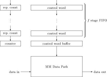 Figure 5: A FIFO for compensating the clock rate difference solution is to add a FIFO between the pads and the control word buffer [see figure 5]. Inserting NOPs in between an atomic sequence can be prevented by preceding each atomic sequence with an externally inserted NOP as the control word, and a repeat count big enough to fill the FIFO with the stable sections of the entire atomic sequence. When the down counter expires, the stages of the FIFO are shifted, and the counter gets the next repeat count as start value. Internally generated NOPs will only reach the MM data path if the FIFO is cleared before the next external control word could reach the control word buffer. Therefore, the depth of the FIFO must not be lower than the depth of the longest atomic sequence. As will be shown in [Section 5.2], analyzing atomic sequences of FastMM* allows for reducing this depth. Page 738 5.1 Atomic Instruction Sequences of FastMM*
For observing the control word flow at the MM data path, a simulation
environment has been developed. This environment uses The use of the procedural simulation interface provided by GENIE has several advantages: - Simulation runs of high complexity can be controlled and evaluated by using a C-like language, thus allowing a higher level of abstraction than with conventional methods. - Straightforward observation of the 696 bit wide MM data path becomes enabled. - One can get the sequence of stable sections (that is, the control words and the associated number of cycles) for a modulo multiplication totally automatic. - Flexibility in controlling the simulation simplifies extracting the atomic sequerrces. - Once the simulation environment is "debugged", the occurance of errors when analyzing the interface is minimized. Using this environment, the control signal interface of the MM data path can easily be analyzed for different algorithms as well as for different implementations of the same algorithm. Additionally, it supplies the control words needed for controlling a test chip which uses the proposed FIFO. 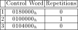  In [Table 2] and [Table 3], the atomic sequences for Mult- We observe that Mod-Mul calls for a FIFO of at least depth 9. This result is only valid for the FastMM* algorithm: as mentioned in [Section 4], the FastMM algorithm would increase depth significantly. ---------------
Page 739 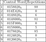 5.2 Reducing Depth of the Instruction FIFO
Having in mind [Table 3], we are able to introduce some
optimizations. Since Mod-Mul starts with a control word which is
repeated many times, this atomic sequence doesn't need to be preceded
by an externally inserted NOP: the FIFO will be filled, anyway. Thus,
waste of execution cycles can be reduced. That is true because we
made the implicit assumption A closer look at [Table 3] shows that for r
= 5 a FIFO of depth 3 is sufficient because within Mod-Mul there are
stable sections long enough to prevent clearing out the FIFO. This
depth also satisfies Mult- A second possible method to reduce the depth of the FIFO is to split the atomic sequence associated with Mod-Mul into three shorter atomic sequences associated with the multiplication steps (A), (B) and (C). This method adds extra cycles to the entire modulo multiplication, but does not lead to a smaller FIFO than the first method does. Because speed of the modulo multiplication is the bottleneck of an RSA implementation, that method is not of prime interest. 6 An Outline of the Hardware Implementation
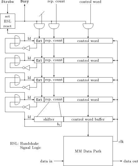
Using a FIFO for controlling the MM data path meets the goal of having an "as simple as possible" control structure for testing purposes. It would be quite consistent to avoid extremely complex design methods when implementing the FIFO in hardware. For the same reason, shifting the contents of the FIFO stages is chosen to be done synchronously rather than asynchronously. The clock of the MM data path is used, since the FIFO must operate at the same (high) speed. This high speed seems to be the only substantial difficulty when designing the FIFO circuit layout. As we have seen in [Section 5], a down counter will be needed. It has to fulfil the given timing constraints: decrementing, detecting underflow, setting up load signals for the stages and shifting the stages must work within a single cycle. Therefore, the down counter is replaced by a shifter, as shown in [Figure 6]. This Page 740 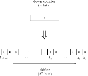 way, much of time is saved because shifting a single bit works a lot faster than decrementing a counter, and no decoder is necessary for detecting whether the next control word has to be loaded: this can be done by inspecting the single bit b0. To avoid an excessively long shifter, its length can be decreased by limiting the repeat count to a certain power of two, thus splitting long stable sections. On the increasing FIFO depth resulting thereof and the length of the shifter a good compromise has to be evaluated. Figure 7 shows a schematic diagram with a FIFO of depth 4. Precise timing issues are omitted: in particular, the circuit for the handshake signal timing has to be designed carefully. Special attention has to be paid to the asynchronous Strobe input to avoid metastable states and synchronization failure. The handshake procedure works in the following way: If the top FIFO stage is empty, Busy is set to low, indicating a request for the next control word. The positive edge of Strobe signals that the next control word is available from outside, and sets Busy to high. For the time Busy is low, internal NOPs with repeat count 0 are to be inserted. This is done by "anding" the input signals with Busy. Additionally, the Ext bit is cleared, indicating an internally generated NOP. If Busy is high and the load signal for the top stage is set, there must have been a rising edge of Strobe (because the load signal resets Busy). In that case, the top stage is loaded from outside. Load signals are generated as follows: Expiration of the shifter means to load all stages. If any stage is marked as an internally generated NOP, it should be overwritten at the next cycle, and all stages above have to move down: with other words, the decision for shifting an upper stage depends on the state of all underlying stages. This results in cascaded OR gates, shown in [Figure 7]. Remember there is only one cycle for setting up all load signals, therefore serious Page 741
delays caused by cascaded gates must be avoided. 7 Conclusion
In order to design a chip for testing the MM data path, we searched a minimum version of the control structure. After analyzing the data flow at the control interface, we introduced a FIFO for compensating the difference of the maximum clock rate allowed by the chip"s pads, and the clock rate the MM data path Page 742 requires to reach the desired encryption rate. Simulation results for a complete 664 bit RSA run based on M-models of the FIFO and the MM data path showed that it is sufficient to precede the whole sequence of multiplications with only a few NOPs, if we use the FastMM* algorithm and do not reduce the depth of the FIFO as described in [Section 5.2]. In this case, not even a single additional NOP needs to be inserted in between that sequence of multiplications. Because almost all cycles of a complete RSA run are needed for that sequence of multiplications, overall performance is not significantly affected by a slow clock rate at the pads. Therefore, if there is no need to reduce the depth of the FIFO (e.g. for shrinking down its size to save chip area), an RSA chip using the proposed control stucture might be appropriate even beyond testing purposes. References
[Knuth 1981], D.E. Knuth: The Art of Computer Programming. Second Edition, Volume 2 / Seminumerical Algorithms, Addison-Wesley (1981), pp 441-442. [Lippitsch et al 1991] P. Lippitsch, K.C. Posch, R. Posch: Multiplication As Parallel As Possible. First International Conference of the Austrian Center for Parallel Computation, (Sep. 1991). [Lippitsch et al 1992] P. Lippitsch, K.C. Posch, R. Posch, V. Schindler: A scalable design with encryption rates from 200 kBit/s to 1.5 MBit/s. 32nd International Science Week, Damascus, (Dec. 1992). [Montgomery 1985] P.L. Montgomery: Modulo Multiplication without Trial Division. Mathematics of Computation, Volume 44, Number 170, (Apr. 1985). pp 519-521. [Posch et al 1990] K.C. Posch, R. Posch: Approaching encryption at ISDN speed using partialparallel modulus multiplication. Microprocessing and Microprogramming 29, (1990), pp 177-184 [Rivest et al 1978] R. Rivest, A. Shamir, L. Adleman: A method for obtaining digital signatures and public-key cryptosystems. Comm. ACM (1978), pp 120-126. [Wallace 1964] C.S. Wallace: A suggestion for a fast multiplier. IEEE Transactions on Electronic Computers, Vol. EC-13, (Feb. 1964), pp 14-17. [Weste et al 1993] N.H.E. Weste, K. Eshraghian: Principles of CMOS VLSI Design. A Systems Perspective. Second Edition, Addison-Wesley (1993).
Page 743
|
|||||||||||||||||
 crypto chip
was designed. It is an architecture capable of performing fast RSA
encryption and other cryptographic algorithms based on modulo
multiplication. Besides the modulo multiplication algorithm called
FastMM, the reasons for its high computation speed are the As
Parallel As Possible (APAP) architecture, as well as the high
operation frequency. The
crypto chip
was designed. It is an architecture capable of performing fast RSA
encryption and other cryptographic algorithms based on modulo
multiplication. Besides the modulo multiplication algorithm called
FastMM, the reasons for its high computation speed are the As
Parallel As Possible (APAP) architecture, as well as the high
operation frequency. The  crypto chip has
been designed to be able to evaluate the behaviour of the pure MM data
path. In the following, we describe the strategies used with the
crypto chip has
been designed to be able to evaluate the behaviour of the pure MM data
path. In the following, we describe the strategies used with the  Crypto Chip, which
has as its core a data path of rather high complexity for performing
modulo multiplications (MM), organized as a bitslice SIMD
architecture [
Crypto Chip, which
has as its core a data path of rather high complexity for performing
modulo multiplications (MM), organized as a bitslice SIMD
architecture [ Crypto Chip, modulo multiplication is done by the FastMM algorithm
[
Crypto Chip, modulo multiplication is done by the FastMM algorithm
[ which is used to calculate the relaxed residuum
 denotes the i rightmost bits of w,
  denotes the i leftmost bits of w):
 : Eight bits, holding the value of
  .
Mult-K: Load register Trp with
.
Mult-K: Load register Trp with  for multiplying with Mkd.
 Crypto Chip, p = 8 has been
chosen.
Crypto Chip, p = 8 has been
chosen. denotes the content
of Reg at the nth cycle: c is a positive constant depending on the
APAP-structure and the adders.
denotes the content
of Reg at the nth cycle: c is a positive constant depending on the
APAP-structure and the adders. , because we assign the correct value to k (in this
context we consider k = 0) and set Mult-K to high for one cycle. This
way, the content of Mkd gets multiplied with one (i.e.,
, because we assign the correct value to k (in this
context we consider k = 0) and set Mult-K to high for one cycle. This
way, the content of Mkd gets multiplied with one (i.e., ), and must
be loaded from the APAP-adder into High at the very right moment,
since the APAP-adder is shifting its content permanently.
), and must
be loaded from the APAP-adder into High at the very right moment,
since the APAP-adder is shifting its content permanently. and Mod-Mul work correctly if
and only if their related sequences of control words appear in a
given order with a given timing: in particular, the control words
within these two operations must not be separated by any additional
control word, not even by a NOP (that is, a control word which
performs no operation onto the MM data path). That is because the
flow of the different data streams will proceed with the internal
clock, and synchronization with external feeding of control words is
to be assumed at given cycles. Obviously, a wrong product would be
calculated otherwise. We will refer to such a non-interruptable
sequence of control words as an atomic sequence. Wef urther note that
throughout the algorithm some control words are repeated several
times. These sections will be referred to as stable sections.
and Mod-Mul work correctly if
and only if their related sequences of control words appear in a
given order with a given timing: in particular, the control words
within these two operations must not be separated by any additional
control word, not even by a NOP (that is, a control word which
performs no operation onto the MM data path). That is because the
flow of the different data streams will proceed with the internal
clock, and synchronization with external feeding of control words is
to be assumed at given cycles. Obviously, a wrong product would be
calculated otherwise. We will refer to such a non-interruptable
sequence of control words as an atomic sequence. Wef urther note that
throughout the algorithm some control words are repeated several
times. These sections will be referred to as stable sections. .
. when performing operation
Mult-
when performing operation
Mult- , thus shifting the multiplier to the left by k bits for
aligning at a desired border. After the modulo multiplication is
finished, a final alignment is necessary to get the correct result.
Furthermore, En-Cut must be able to truncate at arbitrary bit borders
rather than at a position
, thus shifting the multiplier to the left by k bits for
aligning at a desired border. After the modulo multiplication is
finished, a final alignment is necessary to get the correct result.
Furthermore, En-Cut must be able to truncate at arbitrary bit borders
rather than at a position 
 and
and  can be determined to
meet the conditions
can be determined to
meet the conditions  (mod i) and
  (mod
i). Typically, one chooses
(mod
i). Typically, one chooses  , where r is the radix on which
the long integer hardware is operating. The goals defined above can
be achieved by calculating M1, and in the following
way:
, where r is the radix on which
the long integer hardware is operating. The goals defined above can
be achieved by calculating M1, and in the following
way: is always 0,
therefore control signals associated with
is always 0,
therefore control signals associated with  may be omitted.
 for
controlling the simulation of an RSA encryption with
for
controlling the simulation of an RSA encryption with  . The
simulation is based on an functional
. The
simulation is based on an functional  -model of the MM data path.
 and
Mod-Mul of a full 664 bit modulo multiplication are shown. For each
stable section the first value represents the control word, the
second value the required repeat count.
and
Mod-Mul of a full 664 bit modulo multiplication are shown. For each
stable section the first value represents the control word, the
second value the required repeat count. (General Interpreted Environment) is a general-purpose interpreted
language well-suited for use as a control language attached to
application programs like Lsim.
(General Interpreted Environment) is a general-purpose interpreted
language well-suited for use as a control language attached to
application programs like Lsim. design automation tool that allows to analyze the behaviour of
electronic designs ranging from high-level, abstract system models
through full-custom integrated designs.
design automation tool that allows to analyze the behaviour of
electronic designs ranging from high-level, abstract system models
through full-custom integrated designs. is a hardware description
language for describing the behaviour of circuits in functional
models, for use with the Lsim simulator.
is a hardware description
language for describing the behaviour of circuits in functional
models, for use with the Lsim simulator. , where
  is the external
cycle time (the maximum cycle time allowed by the pads), and
is the external
cycle time (the maximum cycle time allowed by the pads), and  is
the internal cycle time the MM data path uses. It seems to be
adequate to assume r = 5.
is
the internal cycle time the MM data path uses. It seems to be
adequate to assume r = 5. .
.