| Submission Procedure |
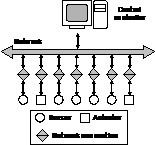
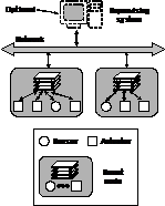
A Modular Architecture for Nodes in Wireless Sensor NetworksJorge Portilla Angel de Castro Eduardo de la Torre Teresa Riesgo Abstract: The growth of sensor networks during the last years is a fact and within this field, wireless sensor networks are growing particularly as there are many applications that demand the use of many nodes, even hundreds or thousands. More and more applications are emerging to solve several problems in data acquisition and control in different environments, taking advantage of this technology. In this context, hardware design of the sensor network node becomes critical to satisfy the hard constraints imposed by wireless sensor networks, like low power consumption, low size and low cost. Moreover, these nodes must be capable of sensing, processing and communicating physical parameters, becoming true smart sensors in a network. With this goal in mind, we propose a modular architecture for the nodes, composed of four layers: communication, processing, power supply and sensing. The purpose is to minimize the redesign effort as well as to make the node flexible and adaptable to many different applications. In a first prototype of the node, we present a node with a mixed design based on a microcontroller and an FPGA for the processing layer and Bluetooth technology for communications. Keywords: Wireless sensor networks, modular architecture, sensor network node, hardware node design Categories: B.5.1, B.6.0, B.7.0 1 IntroductionMeasurement and control of all kind of parameters in several application scenarios raises some problems and design challenges for researchers. Wireless sensor networks appear as a solution, where hundreds or thousands of sensor nodes take measurements from the environment, process the information and communicate this data to the network and to the final user [Zhang, 04]. This field has grown enormously during the last years and it is expected that this trend continues in the future [Hill, 00] [Chong, 03]. Page 328 These networks are composed of nodes with several constraints due to the nature of the wireless sensor network field, like very low power consumption or very low cost and reliability of the nodes. With sensor networks it is possible to improve the measurement procedure since human intervention is reduced almost totally. Usually, developers focused on a centralized architecture for the system (see Figure 1) where the central node acts as the master and the sensors/actuators as slaves. The master takes information from the slaves, processes it and acts consequently. This approach presents several drawbacks like bottlenecks in the central node and high dependence on the reliability of the master. On the other hand, a distributed architecture arises as another approach (Figure 1) [de Castro, 02], in which each node processes locally the signals from sensors, and communicates them to the network. In this context, if a node fails the network continues working. Furthermore, the traffic of information is reduced, because each node can take decisions locally.
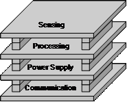
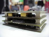
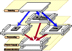
Figure 1: Centralized architecture and distributed architecture of sensor networks As it has been said before, the wireless sensor networks field imposes several constraints to the researchers. Because of this, hardware design of the network nodes becomes critical. This is the point in which this paper is focused. Normally, each application fixes its requirements, and the engineers have to design the system from scratch. This makes redesigning hard and expensive both in terms of time and cost. To solve this problem it is possible to divide the node in functional blocks or layers and so, the redesign effort concentrates in each layer separately. With this approach, it is possible to reuse layers and interchange between different solutions depending on the application requirements. Keeping this idea in mind, a modular architecture of four layers is proposed for the wireless sensor network nodes (Figure 2). These four layers are: communication, processing, power supply and sensing/actuation. Each layer fulfils a specific functionality in the node, and the layers can change between different applications and moreover, it is possible to have an heterogeneous network with nodes composed of different layers. Layers are bonded through vertical connectors which are common to all the layers. As all the layers use the same connectors in the same position, reusability and interchangeability are much easier. Page 329
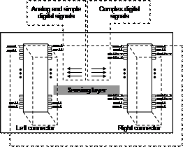
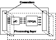
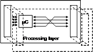
Figure 2 Four layers node architecture and physical aspect of the node 2 State of the art of nodes used in wireless sensor networksSeveral groups work in different hardware platforms for the node in wireless sensor networks, with different conceptions and similarities as well. In the following sections some remarkable work groups' approaches will be described briefly. 2.1 U.C. Berkeley Mica® motesThe Mica mote is an embedded platform composed of an Atmega128 microcontroller from Atmel, a radio module TR1000 from Zeevo and two AA batteries. Moreover, the system has an expansion connector that allows adding different sensor PCBs. The platform runs TinyOS, an operating system created in U.C. in Berkeley as well. TinyOS is an event based operating system in which individual components act together to form a complete application and to implement all system functions [Hill, 02]. There are different Mica models, including versions with ZigBee technology (MicaZ). These motes are commercialized through a company called Crossbow [Crosbow, 05]. Modularity is achieved through a vertical connector allowing the addition of sensor boards to the mote. The connector is a 51-pin vertical connector that allows the addition of different sensor boards depending of the parameters to be measured. In this way, modularity is understood as a two layers architecture, where communication, power supply and processing are fixed, representing one layer. Flexibility is intended for the second layer, which includes the sensors. 2.2 Intel® iMote®The Intel Mote platform includes Bluetooth communications and an ARM core, both in the same chip, a TC200IP from Zeevo. The software architecture is based in the porting of TinyOS to the ARM core [Nachman, 05]. They integrate vertical stackable connectors, in order to make the platform customizable and flexible. In the future, they want to have the sensor board and the power board together in the same system with the main board [Intel, 05], but up to now, they only have one layer (the main board with processing and communications). Page 330 The connectors expose two UARTs, USB, general I/O ports and power, in order to facilitate research. In this way custom sensor boards and debug boards can be attached to the iMote® in a straightforward manner. 2.3 MIT Media Lab modular platformThey have developed a modular platform in which each specific board represents a specific sensing modality (inertial sensing, ambient sensing, etc.). These sensor boards or panes have data collection as their main function [Benbasat, 05]. Their platform is modular as well, with vertical connectors to allow easy combination and recombination of the different panes when the application changes. The purpose is to make a platform as modular as possible, making a general system instead of a specific one. Modularity is applied to the software too, with the intention of have software blocks specific for each pane. The platform includes a master pane, a power regulation pane, a storage pane and different sensing panes depending on the applications. In this way the number of panes is not rigid, and several different panes can be developed depending on the different measures to be taken. The architecture, therefore, implies two fixed layers (master and power regulation) and different possibilities to be added depending on the application. The electrical connections make different signals and power available for the panes. The connectors are two vertical headers of 14 and 12 pins, which are not very robust. 2.4 Tyndall InstituteTyndall Institute developed a platform for wireless sensor networks, stackable and modular. The platform runs an adapted version of TinyOS. On the other hand, the platform can include an FPGA module, for fast DSP processing. They have some sensor layers for different applications and the power supply layer can include batteries or energy harvesting elements. The system incorporates a 2.4 GHz transceiver with a special protocol to minimize power consumption [O'Flynn, 05]. Moreover, they have developed an 802.15.4 compliant layer for communication, in order to have a standard technology in this field. Layers can be interchanged in an easy way, thanks to the vertical connectors, and include communication, processing, sensing and power supply. So they exhibit a four layers design similar to the design presented in this article. 3 Four layers architectureIn this section, the modularity concept and the four layers of the architecture will be detailed. Page 331 3.1 ModularityModularity is an important feature of the node. The purpose is to have a modular platform, flexible and adaptable to several applications and scenarios, and to be able to reuse and interchange between different layers when the application changes. Moreover, the architecture must satisfy several design requirements as it has been said before. To achieve this goal, a four layers modular architecture is proposed. Figure 3: Illustration of modularity With a modular platform new advantages arise, like easy redesigning or the possibility of reusing and interchanging layers (see Figure 3), which reduces cost and time. Furthermore, with this architecture new research possibilities can be tested easily due to the versatility and flexibility of the system. In fact, the node is intended for both research and as a demonstrator of new applications. The modularity is achieved thanks to the vertical connectors. These connectors fulfil the electrical and mechanical connection, and moreover, the logic connection, that is, the connections between the different devices of the architecture (µC, FPGA, sensors, etc.). The connections are fixed in order to standardize the physical architecture of the node. So, it is possible to interchange between different layers, and design new layers in an easy way. Finally, the result is that to interchange between different layers (two sensing layers for example) the only thing to be done is to take out the old layer from the node, take the new layer and insert it in the node, using the vertical connectors. The use of vertical connectors is useful not only to make the mechanical and electrical connections, but to reduce node size, taking advantage of the vertical dimension. This is a trend followed by the different groups in the bibliography, as it was seen in section 2. All these factors make the node very robust and compact. The signals are distributed following some conventions. Assuming that the µC is in the left side and the FPGA is in the right side, the connectors will be called left and right connector. In this way, analog and simple digital sensor signals are connected to left connector pins, as they can be connected directly to the µC. On the other hand, complex digital signals are bonded to the right connector in order to be connected to the FPGA that can easily handle several signals or protocols at the same time thanks to its concurrency (all the logic is executed simultaneously). Moreover, supply and ground signals have been placed in the corners of the connector, as can be seen in Figure 4. Page 332 Figure 4: Distribution of signals and connectors An example of modularity can be seen in Figure 5. There, two different processing layers are shown, one of them with a µC and an FPGA and the other one only with a µC. The first example is a processing layer which should be used in applications which need fast processing or with sensors with complex digital interfaces. The µC deals with simple analog signals and with communications, and the FPGA releases the µC from the tasks related to complex sensors, for example. The second example should be used in applications with analog sensors (the µC has an integrated ADC), or perhaps simple digital sensors, where the µC can face all the work without problems.
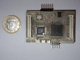
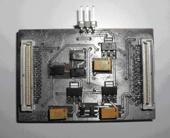
Figure 5: Two different processing layers for different application requirements 3.2 Processing layerThis module provides the smart sensor with intelligence. Here, the signals from the sensors are converted into appropriate digital and processed signals. Moreover, the control of the communications is carried out in this module. Page 333 Searching of neighbour nodes, setting and breaking links, and management of all the tasks related with the network are controlled here by generating commands to the Bluetooth module, and interpreting commands from the Bluetooth module and other network nodes. Power saving modes are managed here too in order to extend the battery life. This is an important matter in wireless sensor networks because it is required that the network works autonomously for a long time without human intervention. A mixed microcontroller/FPGA design is proposed in the first implementation in order to satisfy different requirements for several applications. Versatility is the aim of this election, existing other possibilities such as using the microcontroller only, or the FPGA only. Figure 6: Processing layer hardware 3.2.1 The µCThe µC is an ADUC812 from Analog Devices. This device incorporates 8KB flash memory, 256 bytes of RAM, ADC, DAC, UART and SPI ports, four general I/O ports, and three timers among others peripherals. The µC manages the communications, controlling the Bluetooth module directly through its UART port, and controls the signals from analog and simple digital sensors as well. The clock frecuency in the first prototype is 12 MHz, extendable to 16 MHz. 3.2.2 The FPGAThe FPGA is a Spartan III from Xilinx, specifically an XC3S200 (which integrates 200k logic gates). This device gives the node a big freedom to adapt to new applications, and makes the system versatile in its processing capabilities. The main feature of FPGAs is concurrency. This allows the processing layer to manage complex digital sensors in a fast way, releasing the µC of these tasks. In this context, the µC deals with communication and simple sensors, and the FPGA processes the most complex signals. The FPGA needs three different power voltages, specifically 3.3, 2.5 and 1.2 V. These voltages come from the power supply layer; this point will be commented later on. Page 334 3.3 Sensing layerThis module includes sensors and/or actuators to interact with the environment. According to the use of the smart sensor network, multiple combinations are possible. Multiple kinds of sensors can be included in this level, and actuators may be incorporated as well in order to act according to parameters measured from the environment. In a first application, two different sensor layers have been designed and manufactured. The former is composed of analog and digital sensors, and the latter only includes digital sensors (see Figure 7). This is the first demonstration of modularity in the nodes. The digital version for sensor layer includes an accelerometer and three different temperature sensors. In this way, there are four different signal formats to be processed in the FPGA in order to explore the different interfaces characteristics. In the analog and digital version of sensor layer, sensors of temperature, humidity, infrared and illumination are included. This layer is controlled using both the µC and the FPGA. On the other hand, communications are always managed by the µC.
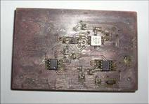
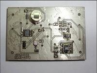
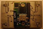
Figure 7: Two sensing layers, with digital sensors and with analog and digital sensors 3.4 Communication layerIn the communication layer a Bluetooth module has been chosen for the first prototype (see Figure 8). This election was done because Bluetooth has low power consumption, enough data rate for the intended applications, it is a widely used technology and works in the 2.4 GHz ISM free license frecuency band. The module incorporated to the node is a OEMSPA13i from ConnectBlue. This module acts as a serial cable replacement. The µC communicates with the Bluetooth module through its UART port. In this way, the module receives simple AT commands from the µC, commands which make the module perform different tasks like search for other modules, establish or break connections, or commands to configure the module, for example. In order to achieve modularity, several communication layers will be considered. With the purpose of deal with the possible interfaces of each wireless module, the µC integrates different interfaces like UART, SPI, and general I/O ports. Page 335 Anyway, the FPGA can solve any problem related to interfacing with the communications layer because it is possible to virtually implement any circuit inside this device. Vertical connectors make this possible, because many signals pass through the communication layer to the processing layer. This point has been taken into account specially to ensure compatibility of the node with future versions of the different layers. Figure 8: Communication layer with the Bluetooth module Other technologies are being studied in order to adapt the module to other application scenarios and to reduce power consumption and network complexity, like ZigBee or a proprietary protocol. 3.5 Power supply layerThis layer generates all the voltages that are needed by the different devices of the node. In the first prototype, the layer takes 5V from an external power supply. With linear regulators the layer supplies 3.3, 2.5 and 1.2 V to the node. These voltages supply the different devices of the node (the FPGA needs the three voltages to work). Inside this layer (see Figure 9) there are the largest capacitors of the node (10 µF), in order to satisfy peak current demands coming from the processing layer. Because of the purpose of having autonomous nodes, different options are being studied in order to integrate new sources like coin cells or AA batteries. In that case, power consumption must be reduced as much as possible. Figure 9: Power supply layer Page 336 4 ApplicationsThe number of applications which can take advantage of wireless sensor networks is huge. This modular solution copes with many different requirements in terms of performance and cost. This technology allows taking measurements from the environment in a way very different from that available up to know. Among these multiple applications we have:
With wireless sensor networks, a new dimension in data acquisition and control arises. A myriad of sensors take measurements from the environment, sometimes in inaccessible places, and process the information, taking decisions if necessary. Human intervention is practically eliminated, and the procedure of measurement improves, although in this aspect node reliability is an important topic. With all these applications fields, it is natural that the sensor networks research area has grown so much during the last years, with several groups researching many topics related to this discipline (communication protocols, power consumption reduction, hardware node design, software, etc.). Inside these different applications, the first framework in which this work focuses is domotics. The measurement and control of parameters in buildings and homes, in order to make life easier and save energy is a strong trend in R & D today. In the future, homes will be full of sensor network nodes, in a non intrusive way, watching everything that happens in the surrounding area. This network will communicate with the PC, a PDA, a mobile telephone or even electrical appliances. Depending on the requirements of the building or home, different implementations of the node can be used. It is possible to have presence detectors, light, temperature, humidity, pressure sensors, actuators to take part in environmental conditions, etc. A set of modules available will be chosen to compose the node. Moreover, if new requirements are imposed, redesign is easy, centering in one layer and more likely in software. This makes the platform very useful and versatile and the reduction of cost is notable. Independently of this first approach, the node is designed to be used in many different applications scenarios, like industries, forests, roads or parkings. The possibilities are unlimited, and modularity helps to adapt the node to all these different situations. Future developments of the prototype will show the benefits and features of the design. Page 337 5 ConclusionsThe increasing importance of sensor networks and, particularly, wireless sensor networks arises new challenges to engineers in several fields. In this context, hardware node design is critical, in order to satisfy hard requirements imposed by the wireless sensor networks field, like power consumption and reduced size. Usually, a change in the application implies redesigning from scratch all the system, which drives to high cost and time inefficiency. So, an ideal solution would be to have a platform that is versatile and adaptable to new situations with minimum redesign effort. A modular architecture for the network node is proposed, in order to achieve these objectives. The architecture is made up of four layers or modules. These layers are communication, processing, power supply and sensing/actuating. A set of these layers is available to create the node for a specific application scenario. Changing of application implies changing the layers or redesigning one or some of them, but in a very easy way. 6 Future WorkThis platform offers a very good opportunity to investigate different aspects of sensor networks. Different cases of study are being considered for future implementations of the node.
References[Benbasat, 05] A.Y. Benbasat, J.A. Paradiso, A compact modular wireless sensor platform, Fourth International Symposium on Information Processing in Sensor Networks (IPSN05), pp. 410 - 415, April 2005. [Chong, 03] Chee-Yee Chong, S.P. Kumar, Sensor networks: evolution, opportunities, and challenges, in Proceedings of the IEEE, pp. 1247 - 1256, August 2003. [Crosbow, 05] www.xbow.com Page 338 [de Castro, 02] A. de Castro, J.M. Chaquet, E.Morejon, T. Riesgo, J. Uceda, A System-on-Chip for Smart Sensors, in Proceedings of the 2002 IEEE International Symposium on Industrial Electronics, vol.2, pp. 595-599, November 2002. [Hill, 00] J. Hill, R. Szewcyk, A. Woo, D. Culler, S. Hollar, K. Pister, System Architecture Directions for Networked Sensors, in Proceedings of the ninth international conference on Architectural support for programming languages and operating systems (ASPLOS00), vol. 34, Issue 5, December 2000, 93-104. [Hill, 02] J. Hill, D. Culler, Mica: a Wireless Platform for Deeply Embedded Networks, in IEEE Micro, vol. 22, Issue 6, pp. 12-24, November-December 2002. [Intel, 05] Intel: Intel Research, Sensor Nets/RFID: Intel Mote, http://www.intel.com/research/exploratory/motes.htm [Nachman, 05] L. Nachman, R. Kling, R. Adler, J. Huang, V. Hummel, The Intel Mote Platform: a Bluetooth-based Sensor Network for Industrial Monitoring, in Fourth International Symposium on Information Processing in Sensor Networks (IPSN05), pp. 437- 442, April 2005. [O'Flynn, 05] B. O'Flynn, S. Bellis, K. Delaney, J. Barton, S.C. O'Mathuna, AM. Barroso, J. Benson, U. Roedig, C. Sreenan, The Development of a Novel Minaturized Modular Platform for Wireless Sensor Networks, in Fourth International Symposium on Information Processing in Sensor Networks (IPSN05), pp. 370 - 375, April 2005. [Power Paper, 05] http://www.powerpaper.com/ [Zhang, 04] Yong Zhang, Yikang Gu, V. Vlatkovic, Xiaojuan Wang, Progress of Smart Sensors and Smart Sensor Networks, in Proceedings of World Congress on Intelligent Control and Automation, vol.4, pp. 3600-3606, June 2004. Page 339 |
|||||||||||||||||||||||||
