| Submission Procedure |
Prototyping on the PC with Programmable Hardware(Department of Electronic and Electrical Engineering, The University, BRADFORD BD7 1DP, United Kingdom jbomar@bradford.ac.uk) (Department of Electronic and Electrical Engineering, The University, BRADFORD BD7 1DP, United Kingdom jmnoras@bradford.ac.uk) Abstract: This paper describes how to design and use a framework of hardware and software for flexible interfacing and prototyping on the PC. The hardware comprises a card with programmable hardware provided by FPGAs, with an interface including DMA block transfer and interrupts. A library of hardware macros is described. Software routines are provided to enable the FPGAs to be programmed and to allow communication between the host PC and the peripheral card. Examples are given to show its use in building and testing designs, so that new applications can be prototyped quickly using a proven and reliable interface. Keywords: Rapid prototyping, PC hardware, PC coprocessor, programmable logic Category: B.6 1 IntroductionThe Personal Computer (PC) environment is used in many application areas, with a multitude of software tools for electronic designers, manufacturers and educators. As the choice of available software grows, at the same time the power of hardware is continually expanded by advances in silicon technology, with market forces driving down prices. However, the performance of standard software platforms can be surpassed by developers turning out low cost customised combinations of hardware and software, as accelerators, coprocessors and preprocessors within PCs. The availability of sophisticated but inexpensive programmable hardware is a major factor in the affordable design and construction of such units. Thus the ability to design reliable custom systems, with performance that would have seemed out of reach a short time ago, is no longer an expensive and rare activity, but increasingly a basic and essential skill. In this paper we describe a flexible prototyping environment using Field Programmable Gate Arrays (FPGAs), primarily directed at the development of PC-AT peripheral hardware for testing and running high-level applications. The paper is Page 86 written for designers intending to build their own custom application cards, so the hardware and software design is described in detail sufficient for it to be adopted easily. To validate our work we have designed and tested a PC-AT card, with a library of configurable hardware elements which can be programmed into FPGAs, and a library of software subroutines for data transfer and control. Together, the two libraries allow standard 8-bit and 16-bit input-output and also Direct Memory Access (DMA) block transfer and interrupt communication between the card and host PC. Because the hardware has in-circuit reconfigurability, it is relatively easy to prototype electronic designs: progress in testing is fast and reliable because the interface hardware and software are known in advance to be correct. 1.1 ObjectivesThe system is proposed as a springboard for rapid prototyping, enabling users to go straight to the heart of their particular problems without first having to study the details of PC interfacing. Subsequent work, for example in optimising an application, might call for deeper knowledge of the interface, but by then users would have some confidence about the main task in hand. Designs are testable from the PC host in a flexible way and at realistic clock and data rates, which is a major advance on static testing. There are existing hardware systems for the construction of simple designs using wire-wrapping, some with programmable chips, and there are also software-oriented systems for specialised applications such as preprocessing of data or images using standard DSP chips. Here we present a development framework with a predetermined but flexible hardware interface to the PC-AT Industrial Standard Architecture (ISA) bus, setting out clearly defined mechanisms for adding in custom or commercially available hardware and high-level software routines. The framework provides:
Page 87
1.2 Structure of the PaperFirst we review previous related work and existing systems. In [Section 3] we clarify our system's specifications and design details, both hardware and software. Next construction and testing are described, and finally we discuss two applications. 2 ReviewPC cards with data processing capability are extensively used for communications (fax, compression or modem), in data capture applications (commonly with DSP hardware) and in a wide range of available products. In this review first we cover briefly a range of research into the potential of PC-based peripheral systems for design prototyping, for computing and signal processing and for educational purposes. We then look at existing commercially available systems, finally suggesting that our system fills a gap in facilities for the high-level development of PC peripherals. 2.1 Application AreasAlthough microprocessors are becoming cheaper and more powerful, many algorithms do not map efficiently onto the architectures and instruction sets of standard processors; for example, some problems lend themselves to pipelining. Thus in many cases the greatest throughput of data requires custom hardware. Hardware built in the past from discrete logic chips, using multi-layer boards to solve layout and timing problems, nowadays can be mopped-up by single chips of programmable logic. Efficient design and simulation tools make it possible to tackle complex problems, and design errors need not result in expensive re-work, as logic is reprogrammable. The following paragraphs offer examples of projects that have combined standard and programmable chips in a range of research and development areas. 2.1.1 PrototypingAs the complexity of chips increases, designers are turning to programmable logic for prototyping, to check functional behaviour and, equally critically, to find out if interface requirements have been captured correctly in the design specification [Quickturn Design Systems 1994], [Maliniak 1996], [Whiny 1996]. Often these prototypes, which save time and money as they avoid the expense and delay of silicon foundry work, are not as fast as the final hardware: however, continual improvements in clock speed and available gate density allow FPGAs to displace standard gate array Page 88 chips in a range of products [Bursky 1995a], [Bursky 1995b], [Bursky 1996]. For the most rapid execution of specialised data-processing algorithms requiring sequences of operations not available directly within standard DSP chips, custom chips are sometimes essential; prototyping of novel DSP systems is an important area for programmable logic [Isoaho et al. 1993], [Isoaho et al. 1994]. Communications hardware is another where the rapid reconfiguration of prototypes is vital, especially with complex or ill-defined interface protocols. Hardware may be for research, or for testing before full-scale production [Kempa and Rieger 1994]. Large systems can be investigated using arrays of programmable hardware on multiple boards. This method is used to explore hardware-software co-design of systems where the initial requirements do not make clear whether the required functions can be most efficiently achieved in hardware, or software, or a mix of both [vom Bögel et al. 1994], [Benner et al. 1994], [Conner 1996], [McIver 1996]. Further examples of rapid prototyping by these means include FIR filter design [Njølstad et al. 1994], a vector graphics controller and a bit-serial DSP processor [Turner and Graumann 1995]. 2.1.2 Computing and Signal ProcessingThe above examples mainly concern single chip designs. Although their individual functional testing is aided by development in a high-level environment, many complete systems are likely to have more than one chip. Several authors have looked at the prototyping of systems combining DSP chips and other hardware for logic and memory functions, used for high-performance signal processing or specialised computing. A list of FPGA-based computing machines is kept on the Internet [Guccione 1996]. Some particular systems are mentioned below. Parallelised applications requiring algorithm-specific architectures may map efficiently onto FPGA arrays. Examples include an image preprocessor for a time-critical avionics application [Lazarus and Meyer 1993] and a Monte Carlo processor to simulate cellular automata systems for use in statistical physics calculations and image-processing [Monaghan 1993]. Authors have also proposed flexible and powerful platforms for general coprocessors: an Sbus workstation coprocessor [Koch and Golze 1994], a word-oriented reconfigurable datapath processor for a Sun SPARCstation [Hartenstein et al. 1994], a real-time image processor built on the SPLASH-2 Sbus attached processor [Athanas and Abbott 1994], the CLP (Configurable Logic Processor) VMEbus machine vision processor [Dunn 1995], the TERAMAC (Tera, or 10 12 , multiple architecture computer) [Snider et al. 1995], and the WILDFIRE prototyping system [Bains 1996]. These systems give some idea of the potential of reconfigurable computing hardware. Other recent proposals include the GRAPE-II system with design entry by dataflow graph [Lauwereins et al. 1995] and a review of the use of the latest SRAM-based Page 89 reconfigurable FPGAs (RFGPAs) for CISC and massively parallel computing [Seaman 1995]. 2.1.3 Educational UsesSince programmable devices first appeared they have been used as a fast and inexpensive way of giving students hands-on experience. Because hardware can be produced without the lengthy delays and expense of external silicon foundry services, complete exposure to the design process from initial idea to hardware testing is possible. The fast and sophisticated chips available now allow the rapid production of complex systems, giving scope to study advanced systems with novel architectures, even within the timescales and budgets of student projects. There is increasing use of programmable logic to explore custom VLSI microprocessors, instruction set design and hardware synthesis [Sandell 1993], [Mat and Noras 1994], [Boerno et al. 1994], [Schubert et al. 1994], [Lam 1994], [Gehrig et al. 1994] and [Bouldin 1995]. 2.2 Existing SystemsUsers who wish to build and test their own systems with field programmable logic now can benefit from a wide range of published ideas and from commercially available products; for example, see [Camerota and Rosenberg 1994] and [Clapp and Harman 1994]. The review above points out many systems that can be copied or adapted for rapid prototyping. A brief discussion of some others, from the small-scale single chip demonstrator board supplied by Xilinx to the Anyboard multiple FPGA prototype card for system design projects, is given by [Pottinger and Eatherton 1994]. The following two sections describe available commercial prototyping products, categorising them as sophisticated hardware for system development, or basic wire-wrapping cards. 2.2.1 Commercial Prototyping SystemsFPGA technology, coupled with interconnect technology [Horng and Sathe 1994], [Mohsen 1993], [Thame 1994a], [Thame 1994b], has made possible hardware prototypes for efficient, high-speed emulation of large digital systems and ASICs, for example during the INTEL Pentium development. FPGA-based hardware emulators have evolved from the first generation which required some manual interconnection through wirewrapping and cabling, to the current second generation using programmable interconnection devices and variable hardware resources. RPM from Quickturn, MARS from PiE and VA-I from Integrated Circuits Application Limited (INCA) are examples of early FPGA-based hardware emulators while ENTERPRISE from Quickturn, VA-II from INCA and APTIX from Aptix are examples of the current generation [Owen et al. 1994]. Virtual Computer is a framework of FPGAs Page 90 and programmable interconnect which, with software compilation tools to translate algorithms into hardware, aims "to provide supercomputing performance to every desktop workstation for a fraction of the cost of supercomputer prices" [Virtual Computer 1994]. 2.2.2 Breadboarding SystemsSeveral hardware aids are available for the development of cards to sit on PC (and other) busses [Amplicon 1996], [Farnell 1995], [Fairchild 1995]. These require wire-wrapping or other manual interconnection to join the bus signals on the card to custom circuitry added by the user. In small or one-off projects, these are most useful in coping with the initial difficulty of getting the basic card to host interface to work correctly and reliably. 2.3 Present Design ObjectivesThe PC prototyping system described in this paper was developed as a framework for rapidly prototyping PC-AT hardware. Designs, down-loaded into FPGAs, perhaps with some modification to the PCB, can be prototyped and tested using the PC host at realistic clock rates. This is not a new idea, but our paper attempts to make the method accessible easily to a wide community of users, by exploring details of the hardware and software required. Also, we suggest a reliable style of interfacing users' designs based on handshaking. Thus, users can be spared the time required to clarify interfacing details, instead being able to concentrate on their applications, and can have more confidence in testing because the basic interface is viable. Our system is not suitable for large circuits which would require more than the hundreds of logic gates within a few FPGAs [see Section 6.1]. Also, we use manual design partitioning and fixed interconnect on the PCB, with a "local" bus running between the FPGAs: users must connect their internal FPGA modules to this bus by wiring up to particular pads. These limitations are consistent with our aim that the framework is mainly for the kind of small-scale application that an inexperienced designer might consider taking on, for example in making the first moves away from designing on PCB with discrete devices, en route towards large designs involving gate-array or ASIC. Previously we built PC prototyping cards to explore the use of FPGAs in replacing many discrete digital IC components and supporting reliable and extensive student projects [Mat and Noras 1994], [Trakas 1994]. With these we can transfer data between card and PC in 8-bit or 16-bit word lengths, with 16 kBytes of static RAM chips and a 40 MHz crystal oscillator clock on the board. Interface routines written in C++ were menu-driven for easy demonstration and use in undergraduate projects. For general prototyping use, a PCB template was provided. Users add new devices and Page 91 tracking into the template file and adapt the PC code supplied to implement and test their own systems. The work described here extends this to support the remaining AT bus interface functions, namely DMA and interrupt functions, excluding only 8-bit DMA transfer. We show below how to achieve all or any of these functions simultaneously. General use requires libraries of software routines and hardware macros, from which designers select those required for their application. 3 System DesignFirst the design requirements and a top-level outline are given and then a summary of the use of Altera and Xilinx devices in the present project. After these initial explanations of the processes and activities involved in the work, more detailed accounts of the software and hardware design are set out. The hardware macro library is fully described in [Section 3.6], and finally how users would build applications on the framework is given in [Section 3.7]. 3.1 Detailed RequirementsThe card has the following basic features: The I/O base address can be selected using a 4-bit DIP switch on the
card. The card also allows all or any of the following features: 8-bit or 16-bit data transfer to and from the host PC. To test the functionality of the interface we include static RAM on our development card. Also we include two FPGAs although only one is essential, as this allows us to demonstrate how to build more extensive designs on this platform. 3.2 Outline DesignA prototype card was designed and developed, containing: Page 92 Two Xilinx XC3042 FPGAs.
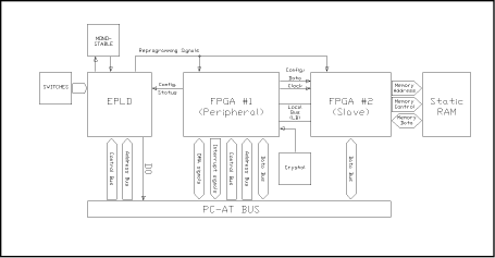
The EPLD, monostable and DIP switch handle address decoding and provide the mechanism for configuring the FPGA chips. This is necessary because initially the FPGA chips have no function until they are programmed. The Xilinx chips contain the rest of the interface and also have uncommitted logic that can be used for custom designs. 3.3 Field Programmable TechnologyGeneral information about the technology of field programmable logic, design methods and applications are found in several helpful publications [Rose et al. 1993], [Bolton 1990], [Chan and Mourad 1994]. Internet information on particular products is available at http://www.actel.com, http://www.altera.com and http://www.xilinx.com. For more general information see http://www.mrc.uidaho.edu. Two papers concentrating on Xilinx devices are [Fawcett 1994a] and [Fawcett 1994b]. In the following, we assess the usefulness of Altera EPLDs and Xilinx FPGAs for our required design functions. 3.3.1 EPLD DesignPage 93 The EPLD chip, Altera EPM7032 [Altera 1993], is an erasable CMOS EPLD that uses EEPROM to set logic functions. It has 600 usable gates and up to 36 inputs or 32 outputs. Because it is involved in the card addressing, it must be programmed before mounting on the PCB. Later, if design changes demand that the chip be reprogrammed, this must be done during temporary removal from the PCB. For address decoding, the chip is connected to nine address lines (A1-A9) and four control lines (RSTDRV, AEN, /IOW and /IOR). A0 is not used for addressing, but together with SBHE it shows whether data being transferred is upper byte, lower byte, or 16-bit [Eggebrecht 1990]. For configuring the FPGAs two outputs go to DONE and /RESET of both FPGAs, while one line goes to READY of the lead FPGA only and another connects with /INIT of the slave FPGA (see [Section 3.3.2] and [Section 3.5] below). Other pins are connected to the 4-bit DIP switch, hard reset switch and the monostable chip. For design entry and realisation, we use Altera's Multiple Array Matrix Programmable Logic User System (MAX+PLUS II) development package [Altera 1992a]. This offers a range of logic design capabilities: a variety of design entry methods, logic synthesis, partitioning, functional and timing simulation, timing analysis, automatic error location and device programming and verification. We chose text entry with AHDL (Altera Hardware Description Language) [Altera 1992b], with a MAX+PLUS II Programmer to obtain a working EPLD containing the design. Part of the circuit inside the EPLD allows the user to set the I/O base address of the card with a 4-bit DIP switch. For designs with A9 = A8 = 1, with A7, A6, A5, A4 set by the DIP switch positions, the I/O base address can be set anywhere between 300 and 3F0 Hex in increments of 16 address locations. A3, A2 and A1 are used to set addresses relative to the base address. The circuit definition in AHDL is given in [Appendix 1]. 3.3.2 FPGA DesignUnlike the EPLD, FPGA chips can be programmed in situ. We use the 3000 family of FPGAs from Xilinx [Xilinx 1994], [Knapp 1996]. These Logic Cell Arrays (LCAs) contain three types of configurable elements: a perimeter of input/output blocks (IOBs), a core array of configurable logic blocks (CLBs) and resources for interconnections. The IOBs provide a programmable interface between the internal logic array and the device's package pins, while the CLBs perform user-specified logic functions. Both IOBs and CLBs contain flip-flops which can store data. To implement a design requires first design capture, then verification by simulation and then mapping to a physical layout. The configuration data representing the physical structure can then be loaded (or "down-loaded") into the LCA. Page 94 Circuit design consists of three basic steps: design entry, physical layout and routing, and verification. Design entry can use high-level routes with schematic capture or text, or low-level packages such as Xilinx's XDE. Many designers prefer schematic capture and Xilinx hardware is reachable from variety of systems such as Viewlogic, OrCAD, FutureNet and Cadence: libraries of parts may be basic digital gates and customised sub-circuits built up by the user, or parameterisable modules provided by vendors [Carlstedt-Duke 1995]. Certain aspects of design are better done with a low-level graphics editor, such as XDE, but normally only by experts. The Xilinx Netlist Format (XNF) is an intermediate design description, in a .xnf file, connecting design capture and software packages for verification and hardware programming. Design implementation is the step where the design's .xnf file is converted by routines XNFMAP and MAP2LCA, which translate the XNF logic representation into a definition of how the hardware in an LCA will be programmed. It is often advantageous to check critical timing and verify functionality of a design before the design is placed and routed into the LCA configuration. This step is the first stage in design verification, using functional and timing simulation, before down-loading and testing the hardware. LCAs are configured by loading data into their on-chip static memory during power-up or when programme mode is enabled. The memory controls interconnection paths for signal routing and logic functions. The memory is static RAM, so the chips are often termed SRAM programmable. At power-up or upon reprogramming, configuration data are loaded into the LCA from an external storage source such as EPROM, RAM or a disk file. Each LCA configuration mode temporarily uses some user-programmable I/O pins for the configuration interface. To configure the FPGA chips on our card, three I/O addresses relative to the base address of the board are used. There is also one address for a general logical software reset, which does not affect the programme of the FPGAs, but restores all their internal flip-flops to a known state. For monitoring of the configuration status of the FPGAs, the READY/_BUSY pin of FPGA #1 connects to the PC through the EPLD. These actions are carried out as follows: Write, base address + 000 (/IOW = 0, /IOR = 1) Reset FPGAs More information about these routines is given in [Section 3.4.1] below. All flip-flops within the FPGAs can also be reset by a switch on the card. The FPGAs' configuration memory can be rewritten to change circuit functions. To initiate reconfiguration, a low pulse lasting at least 6 µsec must be applied simultaneously to the /RESET and DONE pins [Xilinx 1994]. In our card, we produce Page 95 this pulse signal by using a TTL monostable chip and appropriate external
RC timing components. The output pulse length, Tw , is set by
timing components: 3.4 Software DesignAll I/O addresses above 200 Hex can be used by cards in the PC interface expansion slots [Eggebrecht 1990]. Address locations below 200 Hex are used for the base system board, leaving address locations 200 - 3FF Hex available, with some dedicated addresses for the printer port, serial port and so on [Shanley and Anderson 1995]. Although there could be 65,536 unique port addresses, only address lines A1 - A9 are used for I/O decoding, giving up to 512 port addresses. Apart from the three locations mentioned above for device programming and any used by other cards in the PC, all these addresses are available for decoding within the two FPGAs. Two categories of interface software are required to make the card function as required by the user. These are: Utility software for configuring the FPGAs on the card. 3.4.1 Utility Software for Configuring the FPGAsThe Xilinx design route produces a ".bit file", ready to be down-loaded into each target chip. Because our prototype board has two FPGAs and because we wish to have explicit control over the card addressing and data transfer process, we do not use proprietary Xilinx software for device programming. Instead we wrote a routine to preprocess and merge data from separate .bit files, representing the configuration data for each of the two FPGAs, producing a single composite configuration data file called the ".xbm file". This allows users to make independent modifications to the internal designs of either FPGA and then merge the .bit files after verification. The merged file is used by our XIP-XBM programme to load the LCAs configuration data into both FPGA #1 and FPGA #2 on the card, as explained in [Section 3.5] below. However, users can load the configuration data from either .bit or .xbm configuration data files using different software routines. Further details are given in [Section 4.2]. 3.4.2 Application SoftwareWe have developed a small library of routines which users may adopt in their application software, which enable full communication between the PC and the prototyping board. The routines are to enable Page 96 Programmed I/O transfer, These routines must be used in conjunction with macros programmed into the FPGA chips, taken from the hardware macro library described in [Section 3.6]. The software was developed with QuickC and its in-line Assembler. For fuller information, refer to [Omar and Noras 1995]: an example of application software for programmed I/O transfer [Section 4.3.1] is given in [Appendix 2]. 3.5 Hardware DesignFor the two LCA devices we used the Xilinx XC3042, each of which has 144 CLBs in a package with 84 pins. Ten pins are required for control and power functions, leaving 74 uncommitted I/O pins available to the user. FPGA #1 operates in peripheral mode during programming. The PC addresses the LCA and writes one byte of data to it, which is loaded into an internal buffer register. A high on the LCA READY/_BUSY output pin shows that the input register is ready for the next byte. The LCA generates a configuration clock for the internal timing generator and serialises the parallel input data for internal framing and to allow chains of devices to be programmed, data being passed on using the data out (DOUT) pin. FPGA #2 was daisy-chained to FPGA #1 to operate in slave mode, which provides a simple way of loading the LCA configuration data. In slave mode, a lead device (FPGA #1) sends data serially to the slave LCA (FPGA #2) - and clocks its CCLK pin. Most slave mode applications are daisy-chain configurations in which the data inputs are supplied by the previous LCA data outputs, while the common clock is supplied by a lead device in master or peripheral mode. In the next two sections, the functions of the two LCAs are briefly described. 3.5.1 FPGA #1This provides the interface between the card and the PC bus. Ten address lines (A0 - A9), sixteen data lines (D0 - D15), five control lines (AEN, /IOW, /IOR, SBHE and /IOCS16), four interrupt lines (IRQ10, IRQ11, IRQ12 and IRQ15) and seven DMA lines (TC, DRQ5 - DRQ7 and /DACK5 - /DACK7) are connected. If all possible interfacing functions are enabled, then 14 out of 144 available CLBs are needed and 46 out of 74 available I/O pins are used. Many applications will require only a subset Page 97 of these, but for testing we include them all. The remaining CLBs are available for general use. The 40 MHz clock is connected to FPGA #1, allowing users to test the interface or to provide synchronisation on the card. In our prototype, FPGA #1 and FPGA #2 are interconnected by 21 lines of Local Bus. This provides communication lines between the two chips and enables large designs to be partitioned over both LCAs. 3.5.2 FPGA #2 and RAM ChipsAlthough the interface itself does not require a second FPGA, testing fully the prototyping system means that its flexibility and potential for expansion have to be checked. Thus a second FPGA and some RAM are included. These are used also to prove the DMA interface. As shown in [Fig. 1], FPGA #2 is connected to the Local Bus and to the RAM. It is also connected directly to the PC data lines (D0 - D15). The user can use these to transfer data directly between FPGA #2 and the PC data bus, without going through FPGA #1. The two RAM chips connected to FPGA #2 provide local storage for memory- intensive design. They can provide 8k x 16-bit storage and all their addresses, data and control lines are connected to FPGA #2. The user can control and use this RAM by mapping an appropriate design onto FPGA #2. When small amounts of RAM are required, it is possible to integrate this using either FPGA [Xilinx 1994]. However, RAM-based programmable devices from Xilinx are a very inefficient substitute for conventional memory when the amount required is large. 3.6 Hardware Macro LibraryWe have developed a number of hardware modules for general addressing, control and data bus interface, which can be programmed into the FPGAs. The Cadence design system is used to place them within designs symbolically, subsequently compiling the .xnf files for each FPGA. Fuller details, including schematics of the parts described are available [Omar and Noras 1995], but the verbal descriptions given below should be enough to demonstrate the problems associated with interfacing hardware to the ISA bus. Enough information is given for users to be able to reproduce or adapt our solutions. In the following paragraphs, we use the prefix "X" on signal names to identify the primary bus signals; for example, XSBHE is a bus signal, while SBHE is the buffered version to be found on the card. The presentation concerns single cycle 16-bit data transfers; 8-bit single cycle or 16-bit double cycle transfers are not covered. Page 98 3.6.1 General Addressing and ControlThe macros described next are essential for communication between the PC and registers or devices on the card. 3.6.1.1 AddressBusThis module connects external signals XA0-XA9 and XSBHE from the PC Address Bus to other user interfaces in the FPGA, such as the AddressDecoder module. The outputs from this module, A0-A9 and SBHE, are buffered versions of the bus inputs XA0-XA9 and XSBHE. 3.6.1.2 AddressDecoderThis module decodes address lines from the PC Address Bus, via the AddressBus module, to address I/O port locations. The users can set which base address they are using between 300 to 3F0 Hex in steps of 16 address locations, by setting inputs A7IN, A6IN, A5IN and A4IN of this module high or low. For example, if all four of these signals are connected to ground, the select line CS0 represents address 300 Hex. Since the PC address line XA0 is not used for decoding, CS7 represents address 30E Hex. If A5IN and A4IN are connected to logic high while A7IN and A6IN are held low, then CS0 represents 330 Hex and CS7 represents 33E Hex. All outputs from the module, CS0-CS7 and CS, are active high. CS is high if any address is correctly decoded, that is if any one of CS0-CS7 is high. If more than one of these blocks is used in order to permit more than eight port addresses, then the separate CS signals from each block should be ORed to form a new global signal. 3.6.1.3 ClockSignalThis module connects the clock signal from the external 40 MHz crystal. It uses the internal Xilinx clock buffer for minimum-skew clock distribution with no need for further buffering. All synchronous elements should use this clock directly without gating. Xilinx provide flip-flops in the XC3000 library with a reliable, glitch-insensitive internal clock-enable for designs which require that feature. 3.6.1.4 ControlSignalThis connects XAEN, XIOW and XIOR signal lines from the PC Bus to logic within the FPGAs. Output AEN from this module has the same sense as input XAEN while Page 99 outputs WR and RD are active high, rather than active low; we have preferred to keep all card signals consistently active high as a convention. 3.6.1.5 IOCS16This module supplies the XIOCS16 signal to the PC bus for any valid address decode, to indicate that the card supports 16-bit data transfer. 3.6.1.6 MuxOutBusThis multiplexes two 8-bit signals from its A0-A7 and B0-B7 input to its DO0-DO7 output. Supplying logic high at its SELA input will connect A0-A7 to DO0-DO7. Xilinx XC3000 devices do not contain many internal tri-state drivers, so registers must be multiplexed onto the output pins using such a module. To allow several registers to be read, a tree structure of multiplexers must be used. 3.6.2 Data TransferNext we present modules to buffer the PC data bus for input or output and to provide data registers. Also, we describe simple status and flag registers, which can be read or set by the PC and which enable control and signalling. 3.6.2.1 DataBusHi and DataBusLoThese modules interface XD8-XD15 and XD0-XD7 signals from the PC data bus. Data is read from the PC data bus to DI0-DI15 lines of the modules while data is written to the PC data bus from its DO0-DO15 lines. Logic high on DOHIENA or DOLOENA input of the appropriate module enables DO8-DO15 or DO0-DO7 to the PC. The enable signals should be formed in the following way: DOHIENA = CS . RD and where CS is the global enable (see the discussion about the AddressDecoder above). See also the discussion about DMA modules in [Section 3.6.4]. 3.6.2.2 DataRegHi or DataRegLoThese can be used to interface DI8-DI15 or DI0-DI7 from the DataBusHi or DataBusLo module to other user interfaces or processes. Data written asynchronously Page 100 from the PC data bus is available synchronously at the DO8-DO15 or DO0-DO7 outputs of the DataRegHi or DataRegLo module, being latched on the trailing edge of the WR signal. 3.6.2.3 StatusRegisterThis register can be used to interface status signals from any process to the CPU. Inputs SN0-SN7 from a process or processes are clocked synchronously to SOUT0-SOUT7 outputs which in turn can be connected to the DataBus module. When the status has been read by the CPU, the process can be notified using ACK0-ACK7 output of the module if the PC writes data asynchronously back through the module's DI0-DI7 input, so providing a simple handshaking mechanism. 3.6.2.4 ReadFlag and WriteFlagThese modules can be used as single flags to show when the CPU has read from or written to an address selected by CSN. The output D_FLAG can be reset when the operation is completed. 3.6.3 Interrupt handling blocksFor requesting a single interrupt through a particular interrupt line, we provide modules Int10, Int11, Int12 and Int15. Interrupt signal XIRQx is activated by supplying a logic high to the module's REQIx input. When the interrupt is serviced, the initiating process can be notified using the module's CLRIx output. This is done by writing a logic high data to a particular I/O port address, CS0. It is the responsibility of the process to reset the interrupt request line after the interrupt is serviced. There are also modules to support multiple interrupts through a single XIRQx interrupt line (up to 8 per bus interrupt line), using MInt10, MInt11, MInt12, or MInt15. Signals for requesting interrupts through a particular interrupt line (XIRQ10, XIRQ11, XIRQ12, or XIRQ15) are fed through the module's REQx inputs. These signals, clocked synchronously from the process to the module's DO8-DO15 outputs, in turn activate the XIRQx line or lines required. When the CPU recognises this interrupt request, it must read the data on the module's DO8-DO15 output to identify the channel or channels requesting interrupt and then service the (multiple) interrupt accordingly. When serviced, a particular channel causing the interrupt request can be cleared by writing data asynchronously through the module's DI8-DI15 input. This data will be transferred synchronously to the module's CLR0-CLR7 outputs. Page 101 3.6.4 DMA blocksHere we describe some macros suitable to establish DMA facilities on a card. These hardware elements are quite simple, the complexity of the process being in the supporting PC software. 3.6.4.1 DMA-TCThis module connects the XTC signal line from the PC Bus to any user interface in the FPGAs. The user can use this signal to monitor the end of a DMA operation. 3.6.4.2 DMA5, DMA6 and DMA7Each of these interface the DMA signal lines (XDRQ5, XDRQ6 or XDRQ7, and XDACK5, XDACK6 or XDACK7) of a particular DMA channel. Together with the XAEN signal and whichever of XIOR or XIOW is required at a given time, the block addresses correctly the I/O port which initiated the DMA operation. A process can initiate the DMA operation by supplying a logic high to a module's REQDx input. When a data transfer has occured, the module signals the process by using its RDMAx or WDMAx output. It is the responsibility of the process to deactivate the DMA request when all data are transferred, which is indicated by a logic high on output TC of the DMA-TC module. When DMA transfers are used, the definition of the output enables for the data bus modules [Section 3.6.2] must be extended. For example, if channel 5 is used to transfer data from the card to the PC, then the FPGA output buffers must be enabled by logical high signals as follows: DOHIENA = CS . RD + RD . /DACK5 and where the inverse of DACK5 has to be used. 3.6.5 Local BusTo allow for expansion we provide two FPGAs on the prototype PCB and supply a local bus of connections between the two. The chip interface modules are X1-LBus0_7, X1-LBus8_15, X1-LBus16_20, X2-LBus0_7, X2-LBus8_15 and X2-LBus16_20, which map to the correct pin locations on FPGA #1 and #2 respectively. Connections can be inputs, outputs or bidirectional. Page 102 3.6.5.1 X1-LBus0_7, X1-LBus8_15 and X1-LBus16_20These interface between FPGA #1 to the Local Bus LB0-LB20 on the card. This Local Bus interconnects 21 wire lines between FPGA #1 and FPGA #2 on the card. The direction of any Local Bus line is programmable. As input it connects signal from X1LBx to LBIx. As output it connects signal to X1LBx from LBOx, in which case a logic high must be supplied to a corresponding LBOENAx input. 3.6.5.2 X2-LBus0_7, X2-LBus8_15 and X2-LBus16_20These are used in a similar way but interface between FPGA #2 to the Local Bus LB0-LB20 on the card. 3.6.6 Prototype PCB memoryFor interfacing RAM on the card, we developed X2-MDataBusHi, X2-MDataBusLo, X2-MAddressBus, X2-MControlSignal and X2-MAddressGen modules. These modules are used within FPGA #2. 3.6.6.1 X2-MDataBusHi and X2-MDataBusLoThese modules interface signals from the RAM's Data Bus MD8-MD15 and MD0-MD7 to logic within FPGA #2. The function is similar to the DataBusHi and DataBusLo modules mentioned in [Section 3.6.2]. 3.6.6.2 X2-MAddressBusThis drives the RAM address lines XMA0-XMA12 from FPGA #2. Input to this module, MA0-MA12, can be generated within FPGA #2, by using the X-MAddressGen module or simply by using an output port to hold data written from the CPU. 3.6.6.3 X2-MControlSignalThis module is used as an interface to supply XMCS1, XMRD and XMWR control signals to the RAM. The input to this module can be generated within FPGA #2 as relevant for the user application. 3.6.6.4 X2-MAddressGenPage 103 This can generate address signals required by the X2-MAddressBus module. This address generator is programmable. The user can set this address generator by writing to its IA0-IA15 inputs (for full 16-bit address), supplying logic high to its AGSET input and then clocking its AGCLK input. The address can be incremented by supplying logic pulses to the AGCLK input. 3.6.7 Application Hardware and Custom Design BlocksOnce the user has a clear idea of the signals available from the interface modules, implementing a design is a matter of building up logic blocks which use these signals for control and communication with the PC. The library elements presented above suggest a design approach based on handshaking. The user should create modules or hardware processes which send out flags when required, either to the PC via interrupt or DMA request lines, or to other processes. The basic structure acknowledges receipt of the signal: the initiating process may or may not pause while waiting for this response, just as the user wishes. This interface is simple and unrestricting and easily supports connections with standard chips, such as DSP or RAM. 3.7 Extendability and PrototypingWith the standard PCB template containing the interface components predefined and the pin-outs of the standard FPGA devices fixed as far as the PC bus interface and internal Local Bus are concerned, building a prototype requires three stages:
We use Boardmaker for PCB design [Boardmaker 1992]. Aspects of the hardware and software design and test are covered in [Section 4.2] below. 4 Implementation and TestingPage 104 This section runs quickly through the main practical tasks that are required to build a system and to check that it is working correctly. 4.1 Support HardwareThe PCX-795 PC/XT/AT Bus Expansion System [Fairchild 1995] provides multiple slots in a separate powered expansion chassis. With completely untested cards we also use a PCL-757 ISA Bus Switch/Extension Card [Advantech 1991], which buffers the card electrically from the rest of the system. This is to avoid the possibility of the PC crashing during testing, because of software or electrical wiring faults. A logic probe and an oscilloscope, together with PC code for producing test signals, were sufficient for debugging the PCB and checking basic device behaviour. 4.2 Implementation DetailsPutting a circuit design in a LCA requires going from the design idea, to entering (capturing) the design on computer and then using CAD software to produce a physical circuit description. This configuration file is then loaded into the LCA and the design is live, ready to be used.
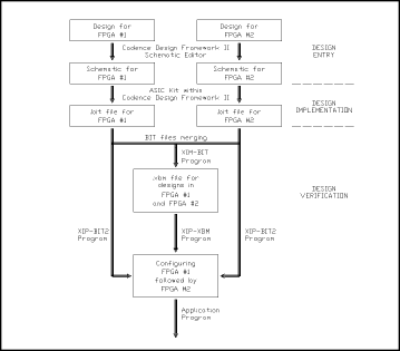
Figure 2: The main steps required to prototype a design. 4.2.1 HardwarePage 105 To map onto the card using both FPGA #1 and FPGA #2, first draw the circuit schematics using Cadence Design Framework II [Cadence 1991], where required connecting the inputs and outputs of FPGA modules to the pre-assigned pads which permit access to the PC bus or the local bus on the card. Then use an ASIC kit targeted at Xilinx, producing separate .bit files for the two devices. This also produces Verilog files for verification by simulation of functionality and timing. 4.2.2 SoftwareTo down-load configuration data into LCAs we use either data from two .bit files or data from a previously merged .xbm file; see [Fig. 2]. Timings for configuration are as follows: on a 286 PC-AT compatible computer with 12 MHz processor speed, transferring separate .bit files took about 0.82 seconds while .xbm files went over in about 0.33 seconds. Thus, for regular use, preprocessing stable design .bit files into a .xbm file saves time. Note that the configuration time is independent of the FPGAs' design complexity; as all CLBs, IOBs and interconnections have to be configured to a stable state whether they are required in the design or not, the volume of configuration data in every .bit file for a given device is the same. Note that the preparation of .xnf files and the allocation of interconnections between FPGAs and any additional chips on the PCB has to be done in advance and manually in our system. With more powerful tools the partitioning of a design to multiple programmable logic chips, often using programmable interconnect, is carried out automatically within the design compilation stages; see [Gokhale and Marks 1995], [Herpel et al. 1995], [Lauwereins et al. 1995], [Schulz 1995] and [Snider et al. 1995]. 4.3 TestingFor initial testing of prototype cards a C routine generates patterns of signals on the PCB, verifying correct addressing and electrical connectivity with the aid of a logic probe and oscilloscope. Once the PCB template is proven, these checks become routine as new applications are developed and the focus switches to using the host PC as test-bed to check for functionality. We developed interface circuits to go in FPGA #1 and FPGA #2, to check data transfers between the PC and registers on the FPGAs and to check transfers between PC memory and the 8k by 16-bit static RAM. There were three main areas to be tested: Programmed I/O data transfer. Page 106 4.3.1 Programmed I/O Data TransferThis circuit is used to test a simple I/O design in FPGA #1 and FPGA #2. Inside each chip we put a 16-bit register to allow the PC to first write and then read back 16-bit or 8-bit data. Inputs of one register are connected to the PC data bus through FPGA #1, while its outputs are connected to the inputs of a second 16-bit tri-state buffer in FPGA #2 via the Local Bus. Outputs of the 16-bit tri-state buffer are connected to the PC data bus through FPGA #2. By sending an I/O read enable signal to this tri-state buffer, any data previously sent to the register can be read back. In FPGA #1 this design used 14 of a possible 144 CLBs and required 50 of a possible 74 I/O pins; in FPGA #2 it took 1 CLB and 35 I/O pins. Software testing showed that this interface circuit functions as expected. 4.3.2 Interface for RAMThis circuit is used to test the RAM chips on the card and verify that the memories are functioning. We address the RAM by writing 13 bits of data from the PC data bus to a 13-bit register within FPGA #2. The chip enable line and read/write control lines are decoded from the PC address and control busses within FPGA #1 and passed through to the RAM via the Local Bus. The data lines of the RAM chips are connected to the PC data bus through FPGA #2. To use the RAM, we have to supply the memory address through the interface circuit within FPGA #2 before writing and reading data to and from the RAM. This design needed 6 CLBs and 20 I/O pins of FPGA #1, and 11 CLBs and 53 I/O pins of FPGA #2. A software routine proved that the circuit functions as required and verified that the RAM can be used correctly. 4.3.3 Interface for Interrupt and DMA OperationsThis circuit is used as an interface between the PC memory and the RAM on the card in which the data transfer between them can be done by programmed I/O transfer, or using DMA or interrupts. DMA requests are generated by writing a command word from the PC to an output port designed within FPGA #1. Data transfer for the DMA operation is done 16 bits at a time. Interrupt requests can be triggered in a similar way, by writing a command word from the PC to another location within FPGA #1. For the DMA operation, all related signals for 16-bit DMA transfers to and from the PC bus are used in this trial, namely DRQ5 - DRQ7, DACK5 - DACK7 and AEN. For the interrupt operation, we tested IRQ10, IRQ11, IRQ12 and IRQ15 signal lines from the PC-AT bus. We can access the card's RAM by programmed I/O operations or using the DMA method. During programmed I/O operation we supply the address Page 107 signals to the memory by sending 13 bits of data from the PC to an output port within FPGA #2. During DMA operations, the address signals to the RAM on the card is supplied by a 13-bit counter within FPGA #2. The circuit decodes all necessary signals during the DMA activity and clocks the counter. The counter can also be reset or set to specific outputs by writing data to an output port within FPGA #2. This design needed 14 CLBs and 46 I/O pins of FPGA #1, and 34 CLBs (26 flip-flops) and 59 I/O pins of FPGA #2. We developed a routine using QuickC to test this interface circuit, using in-line assembler for the interrupt service routines. The functionality of this interface circuit is tested by making a DMA transfer when the interrupt is serviced and looking at both DMA transfer from PC memory to the RAM on the card and from the RAM to the PC, for all DMA channels. We also tested all interrupts. The circuit functions as required. 5 Application ExamplesAs explained in [Section 3.7], prototyping using the card can be done in two ways: use the card as it is and prototype the design using available logic elements in the FPGAs and on-board RAM, or modify the card by adding to the template PCB any additional components required for the new prototype. We describe application examples for these two methods below. 5.1 Using the Unmodified CardBelow two application examples are described, using a 286 PC-AT compatible computer with 12 MHz processor speed. To measure the interface performance, a performance meter was built inside FPGA #1. This is a programmable binary counter driven by the 40 MHz crystal and started and stopped by software commands. Its contents can be written to and read from by the PC, allowing timings for various activities to be measured accurately. 5.1.1 Interrupt and DMA InterfaceThe interface for interrupts and DMA, described in [Section 4.3.3], allows the transfer of data between PC memory and on-board RAM in either direction, using interrupt and/or DMA. This is an example of an I/O interface to FPGA #2. In another example the RAM could be replaced by an ADC and the supporting components needed to build a data acquisition system. Depending on the requirement for the design that we put onto the FPGAs, we may not need to include the circuit for interrupt and DMA, but in this application we used an interrupt to initiate a DMA transfer between the host PC memory and RAM on the Page 108 PCB. Using the performance meter, we find that 8k 16-bit words of data transfer in 16.59 msec. This is equivalent to 980 kBytes per second. Using programmed I/O takes 96.22 msec, a rate of 170 kBytes per second. 5.1.2 2k-block 16-bit AdderThis simple application demonstrates a design of a coprocessor using the card in combination with application software. We use a 16-bit parallel adder [Lenk 1977], controlled by the PC programme. On a START signal initiated by software, the adder carries out 2048 16-bit additions on data located in card RAM. These data are organised in 4 address locations: the first and second locations contain the operand data, the third and fourth locations contain the result of the addition. Data are transferred from the PC memory to the card and then the results are sent back, using programmed I/O or DMA operation. This design used 44 CLBs (42 flip-flops) and 52 I/O pins of FPGA #1 and 109 CLBs (65 flip-flops) and 58 I/0 pins of FPGA #2.
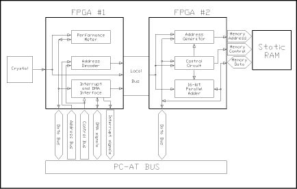
Figure 3: A block diagram of a 2k-block 16-bit adder. The operating speed of the 16-bit adder can be controlled, using a divider to reduce the 40 MHz clock. With a 10, 5 and 2.5 MHz signal clocking the adder, it takes 832, 1651 and 3283 µsec respectively to process the block, in agreement with calculations that the addition should take approximately 819, 1638 and 3276 µsec respectively. The speed of the adder is independent of the PC processor speed. The same 16-bit addition using software on the 12 MHz 286 PC takes 7,276 µsec. With 20 MHz clocking the adder failed to obtain correct results because the RAM had 35 ns access time. Page 109 5.2 Prototyping with a Modified PCBUsing the PCB template of the card, we built a coprocessor card containing a TMS320C25 DSP chip, 8k x 16-bit RAM for DSP program memory, and 8k x 16-bit RAM for DSP data memory, as shown in [Fig. 4]. A relatively simple harness of glue-logic within FPGA #2 is needed to control the DSP and to load and unload its program and data memory. We have used this coprocessor card for processing computed tomography data, using the back-projection algorithm, downloading frequently executed portions of the algorithm into DSP memory for execution by the DSP. Here we used the DSP C compiler to compile the original C code on PC into DSP machine code. For interfacing, i.e to control the DSP and manage data transfer between PC memory and DSP memory, we used many of the hardware macros and software routines previously mentioned.
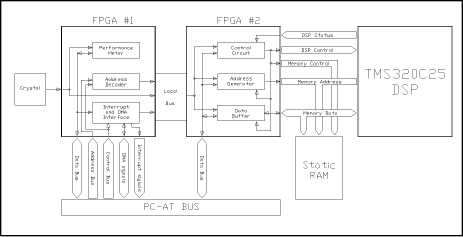
Figure 4: A block diagram of a DSP coprocessor card. The improvement in computational speed is as expected for numerically intensive code running on the DSP chip rather than on the host PC, but overall performance is limited by the amount of RAM on the PCB, with delays due to data transfer bottlenecks. We are looking at the improvements to be got with larger memory on the PCB, and also we are redesigning the system to use dual port RAM for higher throughput. 6 ConclusionsWe have developed a card suitable for prototyping on the PC with programmable hardware provided by FPGAs. A development framework with a predetermined but flexible hardware and software interface is provided. The functionality of hardware Page 110 with appropriate application software has been tested. The card's interfacing features using DMA block transfer and interrupt communication have been shown to work as required. Using various examples, we have shown that it is easy to make a new design and to map it into the FPGAs. The card is ready to be adopted by users to download and test their designs; by modifying it or adding new components, new FPGA-based cards with the same proven interface can be built. 6.1 Limitations of Present SystemThe rapid prototyping tools described in this paper are suitable for small designs [see Section 5.1]. A total of 288 CLBs are provided by two XC3042 FPGAs, with some of these needed for interfacing with the PC bus. However, other FPGAs with higher CLBs per chip, such as the XC3195 with 484 CLBs per chip, can readily be used with slight modification of the PCB template, and FPGAs from later families such as the XC4000 would allow significantly larger designs to be prototyped. More FPGA chips could be added to the card, although the inflexibility of a fixed interconnection scheme and manual partitioning of design onto FPGAs might then start to cause difficulties. Large designs requiring several FPGAs will require design entry using a higher level method such as logic synthesis from hardware description language, rather than schematic capture, and automated design mapping and partitioning tools such as described by [Van den Bout et al. 1992]. The construction of arrays of FPGAs or multi-modules on extensive busses or systolic structures is not feasible with our system: see [Section 2.1.2] and [Section 2.2.1] for references to work in this area. A constraint of the present card, which would inhibit exploitation as a coprocessor, is the small amount of single-port RAM which we incorporated, imposing a bottleneck on data transfer. In principle this limitation can be alleviated by editing the PCB to extend the RAM size; also we are looking at dual-port designs [see Section 5.2]. Further enhancing the data throughput requires moving beyond the ISA bus, as discussed next. 6.2 Further WorkFor applications requiring fast transfer of data, the 16-bit ISA bus has been overtaken by other systems. The most straightforwardly related Extended ISA (EISA) bus has a 32-bit architecture and a different bus-cycle design, which together allow a maximum data-transfer rate of 33 Mbytes/s compared with 8.33 Mbytes/s with ISA. ISA cards can be used with EISA systems. To augment our system to allow full EISA performance is quite feasible, but would require careful consideration. Although the electrical and timing constraints are easy to satisfy with FPGA and EPLD chips, the extended bus has 90 additional contacts - 198 compared with 98 for ISA, and Page 111 requiring a more complex bus adapter. Where the EISA standard was required the additional work on the PCB design would probably require more than a two layer board, whereas ISA needs only two layers. The PCB layout would change extensively, and additional and modified components would be needed in the hardware macro library. The latest system which is receiving great attention at present is the Peripheral Component Interconnect (PCI) bus, which has 32-bit or 64-bit architecture, permitting maximum data transfer rates of 133 Mbytes/s or 266 Mbytes/s respectively [Messmer 1995]. To interface an application board to this bus requires adherence to exacting specifications, both for functionality and timing. At present hard chip-sets are available, and programmable logic manufactures are offering designs for down-loading to FPGA or EPLD which claim to comply with the standard; see references in [Section 3.3] for vendor information. If these are satisfactory, then it would be possible to extend our system to hang onto the end the raw interface devices, using our mechanisms of handshaking, or extending the approach to the use of buffer memory and FIFOs to allow higher data throughput. The sophistication of the PCI standard would make self-design of the basic interface a serious task [Choy 1996]. Again higher density of PCB tracking would be needed, perhaps demanding the use of sub-boards attached to a motherboard. In any case, the details of the software and much of the hardware macros would need to be completely re-cast. However, our general approach should be successful here, as it will be increasingly important to have a secure prototyping framework when working with more exacting and high performance systems. In looking at designing for this interface, we should reformat our libraries to emphasise the elements relating to processes on the PCB and within the FPGAs which are independent of the particular bus employed. Finally, our system could be extended without too much difficulty to allow development and testing of PCMCIA (Personal Computer Memory Card International Association) hardware [Messmer 1995], [Won 1995]. The signals of this interface system are easy to handle once they have been made available at the external socket, that is using a built-in internal PCI/ISA/EISA interface. This is the same strategy as advised in the last paragraph for attaching to the PCI bus. References[Advantech 1991] Advantech Company Limited: "Model PCL-757 ISA Bus Switch/Extension Card: User's Manual"; Advantech Company Limited / Taiwan (1991) [Altera 1993] Altera Corporation: "Altera Data Book"; Altera Corporation / San Jose (1993), 83-88. [Altera 1992a] Altera Corporation: "MAX+plus II: User Guide"; Altera Corporation / San Jose (1992) Page 112 [Altera 1992b] Altera Corporation: "MAX+plus II: AHDL"; Altera Corporation / San Jose (1992) [Amplicon 1996] Amplicon Liveline: "Data acquisition, industrial communications"; catalogue (1996), 6-99. [Athanas and Abbott 1994] Athanas, P. M., Abbott, A. L.: "Image processing on a custom computing platform"; in "Field-programmable logic" edited by Hartenstein, R. W., Servit, M. Z., Springer-Verlag Lecture notes in computer science, 849 (1994), 156-167. [Bains 1996] Bains, S.: "Boards make smarter connections"; New Scientist, 151, 2047 (1996), 21. [Benner et al. 1994] Benner, T., Ernst, R., Könenkamp, I., Holtmann, U., Schüler, P., Schaub, H-C., Serafimov, N.: "FPGA based prototyping for verification and evaluation in hardware- software cosynthesis"; in "Field-programmable logic" edited by Hartenstein, R. W., Servit, M. Z., Springer-Verlag Lecture notes in computer science, 849 (1994), 251-258. [Boardmaker 1992] Boardmaker 2.23: "Boardmaker guide to release 2.23", Tsien Ltd., Cambridge Research Laboratories / Cambridge (1992) [Boerno et al. 1994] Boemo, E., Meneses, J., González de Rivera, G., Barbero, F.: "Field- programmable logic in education: a case study"; in "More FPGAs" edited by Moore, W. R., Luk, W., Abingdon EE&CS Books / Oxford (1994), 452-457. [Bolton 1990] Bolton, M.: "Digital systems design with programmable logic"; Addison-Wesley Publishers Ltd. (1990) [Bouldin 1995] Bouldin, D. W.: "VLSI designer's interface"; IEEE Circuits and Devices, January (1995), 6. [Bursky 1995a] Bursky, D.: "Gate arrays face onslaught of dense and flexible FPGAs"; Electronic Design, June 26th (1995), 85-96. [Bursky 1995b] Bursky, D.: "FPGAs and dense EPLDs challenge gate arrays"; Electronic Design, July 10th (1995), 69-80. [Bursky 1996] Bursky, D.: "Enhanced FPGA family delivers 125,000 gates"; Electronic Design, January 26th (1996), 141-142. [Cadence 1991] Cadence.: "Design Framework II Reference Manual"; Cadence Design Systems (1991) [Camerota and Rosenberg 1994] Camerota, R., Rosenberg, J.: "Data acquisition design with cache logic"; Electronic Product Design, February (1994), 55-56. [Carlstedt-Duke 1995] Carlstedt-Duke, T.: "LPMs cut cost of high level design"; Electronic Product Design, October (1995), 30-39. Page 113 [Chan and Mourad 1994] Chan, P. K., Mourad, S.: "Digital design using field programmable gate arrays"; PTR Prentice Hall / New Jersey (1994) [Choy 1996] Choy, G.: "The PCI wait state challenge"; Components In Electronics, October (1996), 24-25. [Clapp and Harman 1994] Clapp, A. E., Harman, T. L.: "Combining microcontroller units and PLDs for best system design"; IEEE Micro, April (1994), 70-78. [Conner 1996] Conner, D.: "Reconfigurable logic: hardware speed with software flexibility"; Electronic Design News Europe, July (1996), 15-23. [Dunn 1995] Dunn, P.: "A configurable logic processor for machine vision"; in "Field-programmable logic and applications"; edited by Moore, W., Luk, W., Springer-Verlag Lecture notes in computer science, 975 (1995), 68-77. [Eggebrecht 1990] Eggebrecht, L. C.: "Interfacing to the IBM Personal Computer: Second Edition"; SAMS / Indiana (1990) [Fairchild 1995] Fairchild Limited: "Total solution for PC-based industrial and lab automation"; Advantech catalogue, 31 (1995) [Farnell 1995] Farnell Components: "IBM compatible hardware expansion"; October '95 to March '96 catalogue (1995), 165-171. [Fawcett 1994a] Fawcett, B. K.: "Tools to speed FPGA development"; IEEE Spectrum, November (1994), 88-94. [Fawcett 1994b] Fawcett, B. K.: "System-integration features and development tools key to FPGA design"; Microprocessors and Microsystems, 18, 9 (1994), 547-560. [Gehrig et al. 1994] Gehrig, S., Ludwig, S., Wirth, N.: "A laboratory for a digital design course using FPGAs"; in "Field-programmable logic" edited by Hartenstein, R. W., Servit, M. Z., Springer-Verlag Lecture notes in computer science, 849 (1994), 385 -396. [Gokhale and Marks 1995] Gokhole, M., Marks, A.: "Automatic synthesis of parallel programs targeted to dynamically reconfigurable logic arrays"; in "Field-programmable logic and applications" edited by Moore, W., Luk, W., Springer-Verlag Lecture notes in computer science, 975 (1995), 399-408. [Guccione 1996] Guccione, S.: "List of FPGA-based computing machines"; to be found at http://www.io.com/~guccione/HW_list.html (1996) [Hartenstein et al. 1994] Hartenstein, R. W., Kress, R., Reinig, H.: "A new FPGA architecture for word-oriented datapaths"; in "Field-programmable logic" edited by Hartenstein, R. W., Servit, M. Z., Springer-Verlag Lecture notes in computer science, 849 (1994), 144-155. [Herpel et al. 1995] Herpel, H-C., Ober, U, Glesner, M.: "Prototype generation of application specific embedded controllers for microsystems"; in "Field-programmable logic and Page 114 applications" edited by Moore, W., Luk, W., Springer-Verlag Lecture notes in computer science, 975 (1995), 341-351. [Horng and Sathe 1994] Horng, C-S., Sathe, S.: "Programmable interconnect in FPGA-based prototyping"; Electronic Product Design, February (1994), 39-43. [Isoaho et al. 1993] Isoaho, J., Pasanen, J., Vainio, O., Tenhunen, H.: "DSP system integration and prototyping with FPGAs"; Journal of VLSI Signal Processing, 6, (1993), 155-172. [Isoaho et al. 1994] Isoaho, J., Jantsch, A., Tenhunen, H.: "DSP development with full-speed prototyping based on HW/SW codesign techniques"; in "Field-programmable logic" edited by Hartenstein, R. W., Servit, M. Z., Springer-Verlag Lecture notes in computer science, 849 (1994), 318-320. [Knapp 1996] Knapp, S.; See http://www.xilinx.com/products/fpgaspec.htm#XC3000 and http://www.xilinx.com/products/fpgaspec.htm#XC4000 [Kempa and Rieger 1994] Kempa, G. J., Rieger, P.: "MARC: a Macintosh NUBUS-expansion board based reconfigurable test system for validating communication systems"; in "Field-programmable logic" edited by Hartenstein, R. W., Servit, M. Z., Springer-Verlag Lecture notes in computer science, 849 (1994), 409-420. [Koch and Golze 1994] Koch, A., Golze, U.: "A universal co-processor for workstations"; in "More FPGAs" edited by Moore, W. R., Luk, W., Abingdon EE&CS Books / Oxford (1994), 317-328. [Lam 1994] Lam, D.: "Educational use of field programmable gate arrays"; in "Field-programmable logic" edited by Hartenstein, R. W., Servit, M. Z., Springer-Verlag Lecture notes in computer science, 849 (1994), 277-279. [Lauwereins et al. 1995] Lauwereins, R., Engels, M., Adé, M., Peperstraete, J. A.: "Grape-II: A system-level prototyping environment for DSP applications"; IEEE Computer, February (1995), 35-43. [Lazarus and Meyer 1993] Lazarus, R. B., Meyer, F. M.: "Realization of a dynamically reconfigurable preprocessor"; IEEE National Aerospace and Electronics Conference / Dayton (1993), 74-80. [Lenk 1977] Lenk, J. D.: "Logic Designer's Manual"; Reston Publishing Company / Reston (1977), 263-273. [Maliniak 1996] Maliniak, L.: "Pin multiplexing yields low-cost logic emulation"; Electronic Design, January 22nd (1996), 65-69. [Mat and Noras 1994] Mat, I., Noras, J. M.: "A development framework for hardware-software codesign, evaluation and rapid prototyping"; Malaysian Journal of Computer Science, 7, (1994), 95-105. [McIver 1996] McIver, A.: "Software, who needs it?"; New Scientist, 2nd November (1996), Page 115 40-43. [Messmer 1995] Messmer, H-P.: "The indispensable PC hardware book: Your hardware questions answered"; Addison-Wesley / Wokingham (1995), 2nd edition. [Mohsen 1993] Mohsen, A.: "Programmable interconnects speed system verification"; IEEE Circuits and Devices, May (1993), 37-42. [Monaghan 1993] Monaghan, S.: "A gate-level reconfigurable Monte Carlo processor"; Journal of VLSI Signal Processing, (1993), 139-153. [Njølstad et al. 1994] Njølstad, T., Pihl, J., Hofstad, J.: "ZAREPTA: a zero lead-time, all reconfigurable system for emulation, prototyping and testing of ASICs"; in "Field-programmable logic" edited by Hartenstein, R. W., Servit, M. Z., Springer-Verlag Lecture notes in computer science, 849 (1994), 230-239. [Omar and Noras 1995] Omar, J., Noras, J. M.: "A practical guide to prototyping on the PC with programmable hardware"; Department of Electronic and Electrical Engineering Internal Report Number 584, University of Bradford, UK (1995) [Owen et al. 1994] Owen, H. L., Khan, U. R., Hughes, J. L. A.: "FPGA-based emulator architectures"; in "More FPGAs" edited by Moore, W.R., Luk, W., Abingdon EE&CS Books / Oxford (1994), 398-409. [Pottinger and Eatherton 1994] Pottinger, H. J., Eatherton, W.: "Using a multi-FPGA based rapid prototyping board for system design at the undergraduate level"; Proceedings of the 37th Midwest Symposium on Circuits and Systems, IEEE / New Jersey (1994), 437-439. [Quickturn Design Systems 1994] Quickturn Design Systems.: "Rapid prototyping systems for early hardware verification"; Electronic Product Design, October (1994), 59-61. [Rose et al. 1993] Rose, J., El Gamal, A., Sangiovanni-Vincentelli, A.: "Architecture of field-programmable gate arrays"; Proceeding of the IEEE, 81, 7 (1993), 1013-1029. [Sandell 1993] Sandell, J.: "Field programmable gate arrays in the undergraduate curriculum"; Proceedings of the 11th Australian Microelectronics Conference / Queensland, October 5-8 (1993), 41-46. [Schubert et al. 1994] Schubert, E., Kebscull, U., Rosentiel, W.: "The use of FPGAs for educational purposes in VLSI microprocessor design"; in "More FPGAs" edited by Moore, W.R., Luk, W., Abingdon EE&CS Books / Oxford (1994), 458-465. [Schulz 1995] Schulz, P.: "Extending DSP-boards with FPGA-based structures of interconnection"; in "Field-programmable logic and applications" edited by Moore, W., Luk, W., Springer-Verlag Lecture notes in computer science, 975 (1995), 78-85. [Seaman 1995] Seaman, G.: "Dynamically reprogrammable FPGAs and parallel computing"; in the British Computer Society's Parallel Processing Specialist Group newsletter "Parallel Update", 18 (1994), 29-37. Page 116 [Shanley and Anderson 1995] Shanley, T., Anderson, D.: "ISA system architecture Third edition"; Addison-Wesley Publishing Company, (1995), 476-489. [Snider et al. 1995] Snider, G., Kuekes, P., Culbertson, W. B., Carter, R.J., Berger, A.S., Amerson, R.: "The Teramac configurable compute machine"; in "Field-programmable logic and applications" edited by Moore, W., Luk, W., Springer-Verlag Lecture notes in computer science, 975 (1995), 44-53. [Thame 1994a] Thame Components Ltd.: "FPID-based communications switching"; part number #D-22-004, May (1994). [Thame 1994b] Thame Components Ltd.: "Programmable switching devices data sheet"; I-Cube document #D-11-004, December (1994). [Trakas 1994] Trakas, P.: "Hardware library for PC interfacing"; Final year project report, Bradford University, UK (1994). [Turner and Graumann 1995] Turner, L. E., Graumann, P. J. W.: "Rapid hardware prototyping of digital signal processing systems using field programmable gate arrays"; in "Field- programmable logic and applications" edited by Moore, W., Luk, W., Springer-Verlag Lecture notes in computer science, 975 (1995), 129-138. [Van den Bout et al. 1992] Van den Bout, D. E., Morris, J. N., Thomae, D., Labrozzi, S., Hallman, D.: "AnyBoard: An FPGA-Based, Reconfigurable System"; IEEE Design & Test of Computers, 9, 3 (1992), 21-30. [Virtual Computer 1994] Virtual Computer Corporation.: "Virtual computer"; P series information sheet 1info1.1, Reseda / California (1994) [vom Bögel et al. 1994] vom Bögel, G., Nauber, P., Winkler, J.: "A design environment with emulation of prototypes for hardware/software systems using Xilinx FPGA"; in "Field- programmable logic" edited by Hartenstein, R. W., Servit, M. Z., Springer-Verlag Lecture notes in computer science, 849 (1994), 315-317. [Whiny 1996] Whiny, H.: "Design experiences on a 41.5 million-gate project"; Electronic Product Design, October (1996), 21-25. [Won 1995] Won, M. S.: "Programmable logic simplifies PCMCIA interface"; Electronic Design, July 24th (1995), 124-126. [Xilinx 1994] Xilinx: "The Programmable Logic Data Book"; Xilinx Corporation / San Jose (1994) SUBDESIGN PLDecod ( AEN, A[9..1], IORn, IOWn, PSTA : INPUT ; Page 117 PGRSTn, RDB00, RSTDRV, SINITn : INPUT ; SWRSTn, SW[4..1] : INPUT ; D0, GRPSELn, PGXILn, PRSTn,RDB00n : OUTPUT; SRSTn, WRB02n, WRB04n, WRB06n : OUTPUT; ) VARIABLE N[10..0], GRPSEL1, WRB000 : NODE ; %_Symbols: ! NOT, & AND, !& NAND, # OR, !# NOR, $ XOR, !$ XNOR_% BEGIN % Address comparator % N4 = AEN !# A3; N5 = SW1 !$ A4; N6 = SW2 !$ A5; N7 = SW3 !$ A6; N8 = SW4 !$ A7; N9 = A8 & A9; GRPSEL1 = N4 & N5 & N6 & N7 & N8 & N9; GRPSELn = !GRPSEL1; % Address decoding % N0 = NOT( !A2 & !A1 & GRPSEL1 ); N1 = NOT( !A2 & A1 & GRPSEL1 ); N2 = NOT( A2 & !A1 & GRPSEL1 ); N3 = NOT( A2 & A1 & GRPSEL1 ); % Write signals % WRB000 = N0 OR IOWn; WRB02n = N1 OR IOWn; WRB04n = N2 OR IOWn; WRB06n = N3 OR IOWn; % Read signal % RDB00n = N0 OR IORn; % For Xilinx Status Reading % D0 = TRI(PSTA, !RDB00); % For Xilinx Configuration % PGXILn = TRI(GND, !PGRSTn); % For Resetting Xilinx Chips % N10 = WRB000 & PGRSTn & SWRSTn & !RSTDRV; PRSTn = N10 & SINITn; SRSTn = N10; END; /* IOTE-nb.C: Testing Programmed I/O design */ #include <io.h> #include <dos.h> #include <stdio.h> #include <conio.h> Page 118 /* Global vars */
#define BaseAdd 0x0370
int PortOut = BaseAdd;
int PortIn = BaseAdd;
/* WritePort(): Function to write word data to output port */
void WritePort(int DataOut)
{
printf(" Value %4x is sent to port number %x \r\n",
DataOut, PortOut);
outpw(PortOut , DataOut);
return;
}
/* ReadPort():Function to read word data from input port */
void ReadPort(void)
{
int DataIn;
DataIn = inpw(PortIn);
printf(" Value %4x is received from port number %x \r\n",
DataIn, PortIn);
return;
}
/* main(): Main programme */
void main(void)
{
int i;
for(i=0; i<30000; i+=5555)
{
WritePort(i);
ReadPort();
}
}
Page 119 |
|||||||||||||||||