| Submission Procedure |
The Price of Routing in FPGAsFlorent de Dinechin Abstract: Studying the architectural evolution of mainstream eld programmable gate arrays (FPGAs) leads to the following remark: in these circuits, the proportion of silicon devoted to reconfigurable routing is increasing, reducing the proportion of silicon available for computation resources. A quantitative analysis shows that this trend, if pursued, will lead to a widening gap between FPGA performance and VLSI performance. Some prospective solutions to this problem are discussed. Key Words: FPGA, reconfigurable computing, routing resources, hardware complexity 1 Introduction1.1 The FPGA success story Any hardware data-processing application requires some kind of dedicated logic circuitry. As a minimum, when using only "off-the-shelf" components, the designer needs some amount of "glue logic" to interface these components together, and to interface them with the rest of the world (be it a computer backplane). But dedicated hardware may also be needed for the bulk of the data processing itself, when no off-the shelf component is available or when their performance is inadequate. Until recently, to implement such dedicated logic, the designer had to choose among the following options:
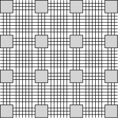
Field programmable gate arrays (FPGAs) were therefore designed as off-the-shelf VLSI circuits able to emulate arbitrary logic, with performances close to those of an ASIC, but with the exibility of software. Typically, a designer evaluates the requirements of his dedicated circuitry (number of gates, number of inputs and outputs, speed), buys an FPGA matching these requirements, and programs it to get an ASIC replacement. The tools used to program FPGAs are very similar to those used to design ASICs (for example they input standard hardware description languages such as VHDL or Verilog), but the designer may Page 227 test his circuit instantly, instead of having to go through the lengthly and costly ASIC foundry process. Besides, some FPGAs are reconfigurable, which allows for hardware debugging and upgrading. Being an off-the-shelf component produced in high volume, the cost of an FPGA in development time is a fraction of the cost of an ASIC. FPGAs have therefore been among the fastest growing sectors of the silicon industry in the last years. They are mostly used as glorified glue logic, replacing ASICs where time to market is critical, or where a small production volume wouldn't justify the cost of an ASIC. Moreover, they have also spawned new applications and research interests, from rapid prototyping of VLSI [SKC + 95] to general-purpose hardware acceleration for numerical applications [Vui94, DeH94, Bre98]. 1.2 FPGA architecturesThe FPGA architecture that allows to achieve these goals typically consists of a large number of configurable logic blocs embedded in a network of configurable interconnections [RM98]. We are not concerned here by the exact nature of the logic blocs (which also contain some memory elements), neither will we discuss the topology of the network, although these two questions have been and still are the subject of abundant research and discussion. We will not escape such discussion later in section 4, but until then an abstracted view of typical FPGA architectures, such as depicted on Fig. 1, will suffice.
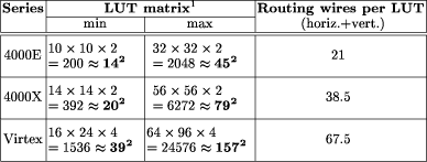
Figure 1: A typical FPGA architecture. Grey boxes are functional units, and lines are wires. To ensure that the interconnect network is programmable, there must be some sort of programmable switch (not shown) wherever two lines cross. What Fig. 1 doesn't show is that the programmability of the FPGAs has a significant hardware cost: there must be switches on the wires to make the Page 228 interconnect network configurable, and there must be some kind of memory holding this configuration along with the configuration of the logic blocks. Finally there must be some dedicated logic and routing to allow for the loading of this configuration. All this consumes a significant proportion of the silicon of a chip, with implications on both capacity and speed of the FPGA. Thus, at a given time, an FPGA built using a state-of-the-art VLSI process cannot hold the biggest full-custom circuits which can be fabricated in the same process. Moreover, for those circuits which are small enough to t in the FPGA, this FPGA implementation is slower than its full-custom counterpart. This cost may be expressed as a time lag between FPGA and full-custom. For example, in 1999, one may observe that top-of-the-range FPGAs from various vendors claim to contain the equivalent of one to two million programmable gates, with system-level operating frequencies above 100MHz. These numbers are comparable with the transistor count (3.1 million, meaning roughly 1 million gates) and the operating frequency (60 to 120 MHz) of Pentium processors built in 1993-1994 : here we have a time lag of five or six years. One may think that this time lag is constant, which would mean that we only need to wait for another ve years to get the current full-custom performance out of an FPGA. The purpose of this paper is to question this assumption: we will show that the current trend in FPGA technology, if pursued, will entail an increase in this time lag. The reason for it is that an ever increasing proportion of FPGA silicon is devoted to the routing architecture, and therefore wasted for computing itself. Therefore the curve of FPGA performance doesn't follow the curve of VLSI integration. 1.3 Rent's rule and FPGAsTable 1 gives a summary of the evolution of routing resources per look-up table (or LUT, the computing unit) in the three most recent FPGA families from Xilinx [Xil97, Xil98]. Figure 2 shows a logical view of an actual recent FPGA, the Xilinx Virtex [Xil98]. This table shows that the amount of routing resources per LUT increases almost proportionally to the number of LUTs per line or column. This general trend [TMM + 98] may be explained by the FPGA version of Rent's experimental law [SKC + 95, Ull84] which states that, as a logic circuit is partitioned, the number of signals crossing the boundary of the partition is proportional to the number of gates on each side, raised to a power r which ranges from 0.5 to 0.8, depending on the class of application. Let us transpose this rule to our FPGA (an extensive review on this kind of problems in the context of FPGAs may be found in section 7.6 of DeHon's thesis [DeH96]). Let us consider a vertical line splitting an FPGA in two halves. If N is the number of LUTs in a row/column, then there are O(N2) gates on each side of the partition. Rent's rule tells that the FPGA needs O(N2r) wires across the vertical line. This line crosses N channels, so we need O(N2r-1) wires per channel. For r between 0.5 and 0.8, the exponent 2r-1 ranges from 0 (constant channel width) to 0.6. However, the value of 2r-1 extracted from Table 1 seems to be quite close Page 229
to 1. This can be explained in several ways:
Whatever the exact growth of routing resources, one obvious consequence is that the proportion of silicon devoted to routing increases with integration. This means in turn that routing has an increasing impact on FPGA performances. This is all the more true as wires, in FPGA, also carry logic: a signal from one gate to another one has to run through the various switches which ensure the programmability of the routing network. This is one major difference when comparing FPGA and full-custom solutions. The purpose of this paper is to study the long-term implications of this evolution. Section 2 will attempt to build a very rough but realistic model of the trend in FPGA technology demonstrated by Table 1. Section 3 then shows that this trend would lead to an increasing performance gap between FPGA and full-custom VLSI. The third section concludes by questioning the model, considering several possible evolutions of FPGA technology which would address the problems exposed here.
1The 4000 series contains 2 LUTs per configurable logic bloc (CLB). The Virtex series contains 4 LUTs per CLB. The LUT matrix is therefore given as (CLBs per line) x (CLBs per column) x (LUT per CLB). Page 230
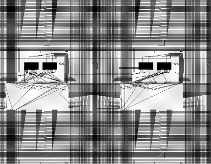
Figure 2: A close-up on Xilinx Virtex chip routing resources in the EPIC tool. The black boxes are computing units, the rest is wiring. Here again, routing switches are not shown, but the white boxes around the computing units are their input/output crossbars. 2 Definitions and hypotheses2.1 Very large scale integrationThe object of our study will be the evolution of FPGA computing power
with respect to VLSI integration. To quantify this integration, we will
use a universal measure, the typical length As we study integration, we will consider circuits of xed size, say square circuits of unit size2. As
2It should be noted that the typical commercial size of a VLSI chip has been almost stable over the decade, at a few square centimeters. For example, the die size of the Intel Pentium II is roughly that of the 80286, even though intermediate processors of the same company have been bigger. In any case, the growth of die size doesn't compare to the growth of 1/  . .
Page 231 will grow as O( This is only an upper bound on computing power: it assumes that all the silicon is used for transistors, whereas in any circuit, you have of course to dedicate some silicon to wires as well. These hypotheses are linked to Noyce's thesis (as cited by Vuillemin
[Vui94]) according to which 2.2 Field-programmable gate arraysLet us now observe a family of theoretical FPGAs which closely follows
VLSI integration: we will note FPGA (
The last assumption may be discussed, considering that technology allows for more and more metal layers to put wires in (current FPGAs use 5 metal layers [Xil98]). The point is, however, that any FPGA wire must have some logic on it: in FPGAs, wires begin and end with switches which ensure the programmability of the routing, and these switches are built out of transistors, and thus consume transistor space. We now need to quantify the number of wires we have in FPGA ( 2.3 A simple model of routingIt is impossible to give a model of all existing and possible routing architectures, therefore we will restrict the study to quantitative aspects. Let N ( Now we have to quantify this increase of routing. Table 1 shows that
routing per channel grows almost linearly with N. We will therefore
consider a number of wires per LUT (in other words a number of wires per
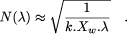
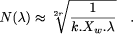
routing channel) which is proportional to N( Page 232 a Rent's exponent of 1. However the same results hold for values of the exponent between 0.5 and 1, as the interested reader may nd in appendix. We choose here to keep the model simple. 3 The price of programmability3.1 Spatial costLet us first estimate N( We now have an idea of the evolution of N(
hence
Lemma 1. The number N( In other words, in order to double the number of LUTs on a row, we have
to wait until 3.2 Time costThe previous analysis also has implications on the maximal operating
frequency of FPGA(
Page 233
Finally, as Lemma 2. The frequency F( 3.3 Peak computing powerAnd finally the peak computing power grows as N( If for example A sensible objection to our study is that we don't compare like for like, as we compare an FPGA with routing to VLSI without routing. This is certainly true: we are comparing peak, or theoretical, computing power. The point is that there exist very efficient architectures with limited or localized routing which, implemented in FPGA, will not benefit from this economy in routing when compared to a VLSI implementation. Consider for example a microprocessor, and suppose that the critical
component of its arithmetic unit is, say, a multiplier. This component
will therefore be heavily optimized for performance. The designers of this
multiplier won't for example allow any external routing channel through
it: external routing will ow around the multiplier (or above if there are
metal layers available). Now imagine the same processor, with the same
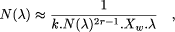
multiplier, implemented in FPGA( This is, once again, probably the main difference between FPGA and full-custom VLSI: in full-custom one pays the performance cost of the routing one gets, whereas in FPGA one pays the cost of all the potential routing even if it isn't being used. 4 DiscussionThis study is not meant to be pessimistic: we trust FPGA vendors for contradicting this dooming view in the forthcoming years. To do so, they just have to contradict one of our hypotheses. Note that, as shown in appendix, taking into consideration a Rent's exponent smaller than 1 doesn't change our conclusion (as long as r > 0.5, which is a prerequisite for an FPGA). 4.1 Constant granularityWe have supposed that the size of the basic building block will remain constant, while their number grows. However it is to be expected that the size of the Page 234 computing unit will grow as well, in order to keep a balance in the routing resources. Note that it is the case in the evolution form the 4000 series to the Virtex series, as the size of the configurable logic bloc has increased from 2 to 4 LUTs. Another example of this trend is Chess [MSK + 99], a reconfigurable array aimed at multimedia applications, where the unit of both computing and routing resources is 4 bits. This architecture is closer in many respects to the MasPar massively parallel computers [HPK95] than to mainstream FPGAs. It is difficult here to resist comparison with the history of parallel computing: the number of processors in parallel computers doesn't grow anymore. Today's biggest parallel computer have no more than a few hundreds of processors, much less than their predecessors of the previous decade (MasPar and TMC computers had tens of thousands). The growth is now in the performance of each processor. We should expect the same kind of evolution in the FPGA world. Exploring this parallel further, let us notice that increasing emphasis, in the parallel computing community, is set on architectural and system techniques designed to hide both the complexity and inefficiency of the communications (e.g. distributed shared memory and caches). Could this trend not lter down to the FPGA world? This is obviously not only a question of architecture. 4.2 Regular architectureWe also expect more and more hierarchy in the FPGA structure [RH97]: near-linear routing is probably not necessary at any scale. Attempts to hierarchical architectures have already been made, for example in the Teramac system [SKC + 95], or in the Xilinx Series 6000 which had a logarithmic routing architecture. The newest Actel FPGAs [KBK + 99] claim to be "semi-hierarchical", with three levels of hierarchy, each level being the usual mesh. However the Xilinx 6000 series was a commercial failure. To say that it was due to its hierarchical routing would be exaggerating: its main weakness, in our sense, was in its vendor place-and-route tools. Altough they were very good at allowing the designer to organize a hierarchy of subcircuits, they were very bad at doing anything automatically. What this example makes clear is that hierarchical routing architectures need sounder bases on the software side to really succeed. This is only one aspect of the evolutions in FPGA support software needed to address the problems shown in this paper. 4.3 FPGA synthesis toolsCurrent FPGA synthesis tools discard the logical hierarchy of a circuit to perform a global optimization of the place and route problem. In the VLSI world, this approach has long been replaced with a more hierarchical one, where a big circuit is decomposed in smaller functional blocks which are then optimized locally (or found in libraries). This doesn't only ease the task of the designer, but also leads to efficient architectures by breaking up global optimization problems into tractable, local ones. Page 235 This point is obviously linked to the previous one: for the hierarchical approach to have the same performance benefits in FPGAs, there must be some form of hardware hierarchy. This was the case in the Xilinx 6000 series. 4.4 General purpose FPGAs, or notSome classes of applications don't need general purpose routing, and would be contented with more scalable architectures. An example is that of datapath-oriented FPGAs, as studied in the Garp project [HW97] among other. Chess [MSK + 99] is dedicated to multimedia processing, and this loss of generality allows for a more efficient architecture in its application eld. An even more radical example is the class of systolic arrays, as obtained using automatic parallelization techniques [Qui84, dD97]: these techniques yield designs with only clock and local routing, which scale well. Could a FPGA family with constant, local routing dedicated to systolic applications be designed? This class of applications, unfortunately, is probably too restricted to make a such a systolic FPGA commercially viable. 5 ConclusionThe increase of road traffic in expanding cities is a fatality for complexity reasons very similar to those presented here. Most big cities have tried to address this traffic increase by widening the roads and increasing the number of lanes. Since the eighties, however, this approach to city traffic is generally considered a failure. One reason is specific to the city metaphor: city planners, unlike FPGA designers, can't move blocks further apart when they want more lanes between them. But even if they could, they would face the citizens' critics: the useful part of the city is the blocks, that is where people live and interact. City-residents are increasingly reluctant to sacrifice this living space to traffic lanes, all the more as they are conscious of the short lifespan of any traffic improvement. Similarly, this study showed that the current evolution of FPGAs gives an increasing proportion of the silicon resources to routing, which is computationnaly useless. It establishes that this trend, if pursued, would lead to an increase of the performance gap between FPGA and full-custom VLSI. The hope is to push long-term researchers to explore alternative possibilities. For example, some cities manage their trafic increase quite well by promoting public transportation (the metaphor of a bigger granularity), local shopping and working (the metaphor for architectural solutions placing the emphasis on local routing), and cycling. Alas, as far as cycling is concerned, we couldn't find an FPGA metaphor. Acknowledgements Special thanks should go to Wayne Luk, Nabeel Shirazi and the ALA team at Imperial College, London, and to Dominique Lavenier of IRISA, Rennes, for many interesting discussions and comments. This work was partly supported by an INRIA post-doctoral fellowship at Imperial College, London, UK. Page 236 References[Bre98] Gordon Brebner. Field-programmable logic: Catalyst for new computing paradigms. In International Workshop on Field Programmable Logic and Applications, Tallin, Estonia, September 1998. [dD97] Florent de Dinechin. Libraries of schedule-free operators in Alpha. In Application Specific Array Processors. IEEE Computer Society Press, July 1997. [DeH94] Andre DeHon. DPGA-coupled microprocessors: Commodity ICs for the early 21st century. In IEEE Workshop on FPGAs for Custom Computing Machines, 1994. [DeH96] Andre DeHon. Reconfigurable Architectures for General-Purpose Computing. PhD thesis, MIT, August 1996. [HPK95] M. Hamdi, Y. Pan, and W. T. Kwong. Effcient image processing applications on the maspar massively parallel computers. International Journal of High Speed Computing, 7(4):489-514, 1995. [HW97] John R. Hauser and John Wawrzynek. Garp: a MIPS processor with a reconfigurable coprocessor. In IEEE Symposium on FPGAs for Custom Computing Machines, pages 12-21, Napa Valley, CA, April 1997. [KBK + 99] S. Kaptanoglu, G. Bakker, A. Kundu, I. Corneillet, and B. Ting. A new high density and very low cost reprogrammable FPGA architecture. In FPGA'99, ACM/SIGDA International Symposium on FPGAs, pages 3-12, Monterey, CA, February 1999. [MSK + 99] A. Marshall, T. Stans eld, I. Kostarnov, J. Vuillemin, and B. Hutchings. A reconfigurable arithmetic array for multimedia applications. In FPGA'99, ACM/SIGDA International Symposium on FPGAs, pages 135-143, Monterey, CA, February 1999. [Qui84] P. Quinton. Automatic synthesis of systolic arrays from recurrent uniform equations. In 11th Annual Int. Symp. Computer Arch., Ann Arbor, pages 208-14, June 1984. [RH97] J. Rose and D. Hill. Architectural and physical design challenges for one-million gate FPGAs and beyond. In FPGA'97, ACM International Symposium on FPGAs, pages 129-132, Monterey, CA, February 1997. [RM98] B. Radunovic and V. Milutinovic. A survey of reconfigurable computing architectures. In International Workshop on Field Programmable Logic and Applications, Tallin, Estonia, September 1998. [SKC + 95] G. Snider, P. Kuekes, W. B. Culbertson, R. J. Carter, A. S. Berger, and R. Amerson. The Teramac configurable computer engine. In Field Programmable Logic and Applications, pages 44-53. LNCS 975, September 1995. [TMM + 98] A. Takahara, T. Miyazaki, T. Murooka, M. Katayama, K. Hayashi, A. Tsutsui, T. Ichimori, and K. Fukami. More wires and fewer LUTs: a design methodology for FPGAs. In FPGA'98, ACM/SIGDA International Symposium on FPGAs, pages 12-19, Monterey, CA, February 1998. [Ull84] Jeffrey D. Ullman. Computational Aspects of VLSI. Principles of Computer Science. Computer Science Press, 1984. [Vui94] Jean Vuillemin. On computing power. In Programming Languages and System Architectures, LNCS 782, pages 69-86, Zurich, Switzerland, June 1994. [Xil97] Xilinx Corporation. XC4000E and XC4000X Series Field Programmable Gate Arrays, November 1997. [Xil98] Xilinx Corporation. Virtex 2.5V Field Programmable Gate Arrays, October 1998. Page 237 A When Rent's exponent is smaller than 1 This section follows the computation of section 3 in the case of a Rent's exponent between 0.5 (constant width channels) and 1. A.1 Spatial cost As exposed in the introduction, a Rent's exponent r corresponds
to a channel width of 2r - 1. The width of an FPGA tile is thus
X l + k.N(
hence
Lemma 3. The number N( A.2 Time cost The period is the sum of:
Let us be optimistic and assume that the routing is good enough for
the period to be limited by the second term in Lemma 4. The frequency F ( Page 238 A.3 Peak computing power And finally the peak computing power grows as N( This result yields the same conclusions with respect to an increase of the time lag between full-custom VLSI and FPGA peak computing power. Page 239 |
|||||||||||||||||
 and 0.1
 1.25 every year. This integration leads to an increase of theoretical computing
power of
1.25 every year. This integration leads to an increase of theoretical computing
power of  2 every
year. Vuillemin concludes from this that the peak FPGA performance also
doubles every year, which we question in the following.
2 every
year. Vuillemin concludes from this that the peak FPGA performance also
doubles every year, which we question in the following.  k.N(
k.N(
 -1/2
=
-1/2
= 
 .
.  ;
; .
As 1/2 < r < 1, we have 0 < 1 -
.
As 1/2 < r < 1, we have 0 < 1 -  <
<  in this case. However this term also assumes a very bad routing architecture,
in which the number of switches on a typical net is proportional to the
size of the chip. This is what you would get on an FPGA with only local
routing, for instance.
in this case. However this term also assumes a very bad routing architecture,
in which the number of switches on a typical net is proportional to the
size of the chip. This is what you would get on an FPGA with only local
routing, for instance.  ).
).